Knowledge Center
This Gold Phoenix PCB Knowledge Center article compares lead soldering and lead-free soldering in the PCBA process, covering melting point, wettability, physical characteristics and the reliability concerns of lead-free manufacturing.
As solder joints in microelectronics devices continue to downsize, they must withstand increasing mechanical, electrical and thermodynamic loads, raising the requirement for reliability. Electronics packaging technologies including SMT (Surface Mount Technology), CSP (Chip-Scale Package) and BGA (Ball Grid Array) technology rely on solder joints to provide electrical and rigid mechanical connections between different materials, so the connection quality and reliability of solder joints determine the quality and reliability of electronic products. Failure of even a single solder joint can possibly cause complete breakdown of an electronic product. Therefore, how to ensure solder joint quality is an extremely essential concern for modern electronic products.
Traditional SnPb solder contains Pb (lead) which, together with lead chemical compounds, is such a highly toxic substance that long-term application will bring extreme damage to people’s life and environment. Up to now, lead-free solder is constantly replacing lead solder for its merits of environmental protection. However, lead-free manufacturing differs from lead manufacturing in the PCBA (Printed Circuit Board Assembly) process, with modified parameters. Therefore, it is of much significance to be fully aware of the comparison between lead soldering and lead-free soldering in PCBA so that electronic products’ performance and functions won’t be compromised by environmental concerns.
Lead-free solder features a higher melting point than lead solder.
a. Melting point of traditional lead eutectic solder (Sn37Pb) is 183°C.
b. Melting point of lead-free eutectic solder (SAC387) is 217°C.
Since lead-free eutectic solder (SAC387) features a 34°C higher melting point than traditional lead eutectic solder (Sn37Pb), the consequences are:
1). The rising temperature afterwards leads solder to be easily oxidized, with chemical compounds quickly growing between metals.
2). Some components, such as those with plastic packages or electrolytic capacitors, tend to be more affected by soldering temperature than other elements.
3). SAC alloy will bring larger stress to components, so components with low dielectric constant will have more access to failures.
4). Numerous types of soldering surfaces are available on the lead-free solder surface of components. Application of tin in solder is more applied due to its low cost. Nevertheless, a thin oxidation layer tends to be generated on the surface of tin. Plus, stress will possibly be made after electroplating. As a result, tin whisker tends to be generated.
Compared with lead solder, lead-free solder features obviously lower wettability. Bad wettability tends to make solder joints perform too incapably to meet requirements in terms of self-alignment capability, tensile strength and shear strength. Bad wettability possibly leads to a higher reject ratio of solder joints when modifications aren’t implemented to compensate for this disadvantage.
The table below demonstrates the physical characteristics difference between lead-free solder and lead solder.
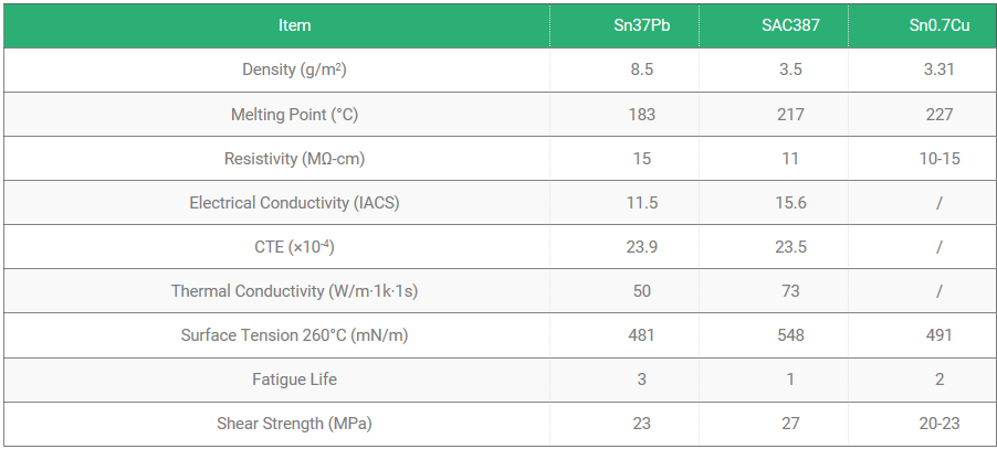
As is depicted in the above table, these differences in solder properties can affect solder joint reliability and require corresponding process adjustments in lead-free manufacturing. From the perspective of mechanical influence, typical lead-free solder is harder than lead solder. Moreover, generated surface oxide, flux contaminant and alloy residue will possibly lead to bad performances on electrical contact and contact resistance. Thus, electronic products’ conversion from lead to lead-free manufacturing is never a pure replacement in either electrical or mechanical aspects, owing to the following reasons:
a. Because lead-free solder joints are generally harder and less ductile than traditional SnPb joints, their mechanical response to stress and thermal cycling can differ and should be considered during design and process control.
b. Because lead-free solder features bad wettability, more defects will be aroused, including voiding, misalignment and tombstoning.
When transforming from lead solder to lead-free solder, the most protruding difference lies in high tin content (>95%Wt). As a result, the following issues should be focused on first.
Tin whisker grows from the weak section of the tin oxide layer as monocrystal tin, appearing in columnar shape or cylindrical filament. Its damages include:
a. Short circuits may be caused between neighboring pins.
b. Bad influence may be generated to high-frequency features.
Pressure stress is available in the tin soldering layer, which is regarded as the essential reason for the generation of tin whisker. For example, when lots of irregular Cu6Sn5 metallic alloy form, a lot of defects will be produced, including pressure stress accumulation on the tin layer, component pin deformation and CTE mismatch, all of which will result in the generation of tin whisker. High tin alloy will lead to the generation of tin whisker, which especially works on pure tin. Lots of metal alloys like Pb or Bi, however, can stop or hinder tin whisker from growing.
Tin whisker possibly causes short circuits on fine-line components, QFP for example. Therefore, pure tin can be plated on low-grade products and components whose life time is less than 5 years. When it comes to high-reliability products and components whose life time has to be over 5 years, a nickel layer should be plated first with thickness less than 1μm, and then comes a tin layer with thickness of 2–3μm.
Metal dendrite features a different growing procedure from tin whisker. The former results from ionic electromigration in electrochemistry. Metal dendrite will lead to short circuits that will further cause circuit failure.
Conductive anodic filament (CAF) is another failure type as a result of electrochemical reaction. CAF takes place inside the PCB board, caused by anode conductive filament containing copper growing from anode to cathode.
CAF grows to an extent when anode and cathode are connected, with short circuits taking place between the two poles, finally leading to catastrophic failure. CAF is a disaster for high-density PCB assembly, and lead-free solder with higher temperature makes this issue happen more easily.
Tin pest results from spontaneous polymorphism phase change of pure tin. When temperature is lower than 13°C, pure tin will convert from white tin (density is 7.30 g/cm3) deriving from a body-centered tetragonal structure to grey tin (density is 5.77 g/cm3) in a cubic structure. Theoretically, tin pest will lead to potential reliability risk, but it is seldom observed because impurity is mixed into tin.
The above discussed issues are possible defects when lead-free solder is applied. These risks can be reduced through appropriate material selection, PCB design, process control and soldering practices during PCBA manufacturing.
Capabilities
Payment Methods


Specials Price
Carriers


Support Hobbyist
Certificate


Customer Support
Follow Us