 Knowledge Center
This Gold Phoenix PCB Knowledge Center article explains PCB voids, including plating voids and solder voids, their causes, impact on circuit functionality, and prevention methods.
PCB voids occur when an un-plated area exists in a circuit board, such as within drilled plated holes, hole barrels, or solder joints. These voids can interrupt electrical connections and affect PCB performance.
There are two main types of PCB voids: plating voids and solder voids. Plating voids occur when copper plating does not completely cover the inner walls of a plated through-hole. Solder voids occur when empty spaces remain inside solder joints due to process-related factors. Both types can affect PCB reliability.
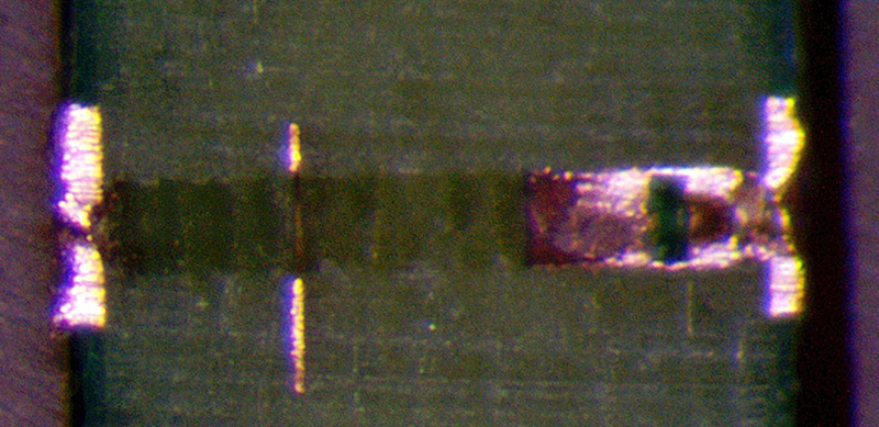
Plating voids are often related to drilling and through-hole preparation. A worn drill bit or unsuitable drilling conditions may create rough or uneven hole walls. During electroless copper plating, copper may not fully cover these imperfections, resulting in non-plated areas.
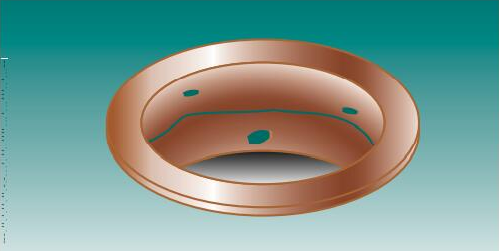
Plating voids can also occur when debris remains inside drilled holes. Contaminants may prevent proper copper adhesion and create areas where plating coverage is incomplete.
Entrapped air bubbles during the electroless copper process can also prevent copper solution from contacting the barrel wall and contribute to void formation.
A solder void is an empty area within a solder joint. Factors that may contribute to solder voids include insufficient preheat conditions, excessive flux, solder paste oxidation, low-quality solder paste, or PCB design characteristics.
Solder void risks can often be reduced by optimizing preheat conditions, using suitable solder paste, and adjusting stencil design.
Both plating voids and solder voids can create manufacturing issues, with loss of conductivity being a major concern.
PCB hole plating provides electrical connections between conductive layers and between the top and bottom surfaces of the board. When voids or un-plated areas occur, current flow may be interrupted, potentially causing PCB malfunction or signal connection issues.
Depending on application requirements and inspection results, voids may require PCB rejection. Preventing void formation is therefore an important part of PCB manufacturing quality control.
Preventing voids depends on identifying the type of void and addressing the related manufacturing process.
For plating void prevention, drilling conditions and hole cleaning processes should be properly controlled. Excessive drilling speed or worn drill bits may create uneven surfaces that are difficult to plate consistently.
Drill bit replacement schedules, drilling parameters, hole cleaning procedures, proper racking, and plating bath control can help reduce plating void risks.
Entrapped air during the electroless process can be reduced through appropriate process control methods.
Capabilities
Payment Methods


Specials Price
Carriers


Support Hobbyist
Certificate


Customer Support
Follow Us








