 Knowledge Center
Types of PCB Pads
1. Common pads
1.1 Square pads - when the components on the printed board are large and few, and the printed wires are simple, they are often used. Using this pad is easy to implement when making a PCB by hand.
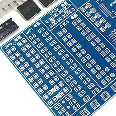
1.2. Circular pads - widely used in single and double-sided printed boards with regular arrangement of components. If the density of the board allows, the pad can be larger, and it will not fall off when soldering.
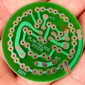
1.3. Island-shaped pad - the connection between the pad and the pad is integrated. Commonly used in vertical irregular arrangement installation.
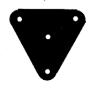
1.4. Polygonal pads - used to distinguish pads with similar outer diameters and different apertures, which are convenient for processing and assembly.
1.5. Oval pads - This pad has enough area to enhance the anti-stripping ability and is often used in dual in-line devices.
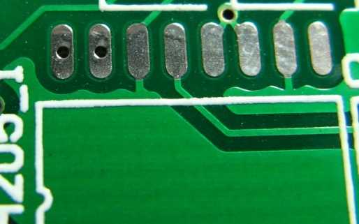
1.6. Open-shaped pads - in order to ensure that after wave soldering, the pad holes for manual repair welding are not blocked by solder.
2. Special pad
2.1. Plum blossom pad
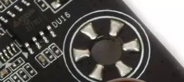
Torx pads are usually used WHERE large vias are grounded. There are several reasons for this design:
1) The fixing hole needs to be metallized and connected to GND. If the fixing hole is fully metallized, it is easy to block the hole during reflow soldering.
2) The use of internal metal screw holes may cause the grounding to be in a poor state due to installation or multiple disassembly and other reasons. The use of plum hole pads can ensure a good grounding no matter how the stress changes.
2.2. Cross-shaped pads
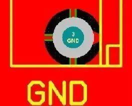
Cross-shaped pads are also called thermal pads, hot air pads, etc. Its function is to reduce the heat dissipation of the pads during soldering, so as to prevent virtual soldering or PCB peeling caused by excessive heat dissipation.
1) When your pad is ground. The cross flower can reduce the area of connecting the ground wire, slow down the heat dissipation speed, and facilitate welding.
2) When your PCB needs a machine patch and is a reflow soldering machine, the cross-hair pad can prevent the PCB from peeling (because more heat is needed to melt the solder paste).
2.3. Teardrop pad
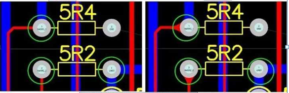
It is often used when the traces connected to the pads are thin to prevent peeling of the pads and disconnection of the traces from the pads. This type of pad is commonly used in high frequency circuits.
Capabilities
Payment Methods


Specials Price
Carriers


Support Hobbyist
Certificate


Customer Support
Follow Us








