Knowledge Center
This Gold Phoenix PCB Knowledge Center article compares ENIG and ENEPIG PCB surface‑finish technologies, including structural features, pros‑and‑cons, black‑pad failure mechanisms, chemical‑reaction principles and practical application guidance.
Among technologies applied in PCB (Printed Circuit Board) fabrication process, surface‑finish treatments play a crucial role in PCB assembly and end‑product electronic performance. Copper layers on PCBs readily oxidize when exposed to air; copper oxidation severely degrades soldering quality. Surface finishes protect copper pads against oxidation to guarantee reliable solderability and electrical performance. Rising market demand for miniaturization, enhanced functionality and improved device reliability drives PCBs toward thinner form‑factors, lighter weight, higher circuit density and faster signal transmission. Accordingly, surface‑finish solutions must meet higher stability and reliability requirements to match these industry trends. Growing global focus on eco‑friendly manufacturing also draws attention to environmental‑impact considerations for PCB surface treatments. RoHS (Restriction of Hazardous Substances) and WEEE (Waste Electrical and Electronic Equipment) regulations issued by the European Union restrict hazardous substances such as lead and mercury within electronic hardware, promoting lead‑free and green PCB surface‑finish manufacturing. As mainstream surface‑finish options, ENIG (electroless nickel immersion gold) and ENEPIG (electroless nickel electroless palladium immersion gold) satisfy modern PCB technical requirements and adapt to lead‑free soldering trends, offering broad application potential.
Nevertheless, many engineers find it difficult to distinguish ENIG from ENEPIG and to identify appropriate selection scenarios. This article defines ENIG and ENEPIG, describes their manufacturing workflows, compares respective advantages and disadvantages, and delivers practical guidance for selecting each surface finish for specific project requirements.
Commonly accepted mainstream PCB surface finishes include HASL (hot air solder leveling), OSP (organic soldering preservatives), Immersion Tin, Immersion Gold, ENIG and ENEPIG. Each surface finish carries distinct strengths and weaknesses. When selecting a suitable surface finish for a given PCB product, key evaluation dimensions include cost, end‑product operating environment, fine‑pitch component requirements, lead‑free or lead‑based assembly conditions, RF high‑frequency performance, shelf‑life targets, shock‑and‑drop resistance, thermal resistance, production volume and throughput.
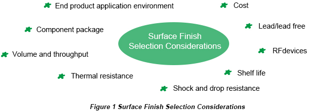
These evaluation items serve as practical references for PCB surface‑finish decision‑making. Note that these factors do not carry equal weight; engineers must clarify priority levels according to specific product conditions.
During the 1990s, as PCB technology shifted toward finer circuit traces and micro vias, together with well‑known drawbacks of HASL and OSP — flatness limitations for HASL and flux‑residue‑removal challenges for OSP — ENIG emerged as an alternative surface‑finish solution for PCB fabrication.
ENEPIG was developed as an upgraded variant of ENIG to mitigate ENIG’s well‑known black‑pad defect. A thin palladium barrier layer (typical thickness 0.05 μm‑0.1 μm) is deposited between electroless nickel and immersion‑gold layers. This palladium layer blocks immersion‑gold solution from corroding the underlying nickel layer, eliminating ENIG‑related black‑pad failures. Beyond black‑pad mitigation, ENEPIG delivers highly reliable wire‑bonding performance, excellent multiple‑reflow soldering tolerance and functional contact surfaces. It satisfies strict requirements for high‑density PCBs assembled with multiple package types, earning it the description of “universal finish”.
ENEPIG‑relevant technology appeared as early as the 1980s; however high material cost and limited industry requirements for advanced surface finishes prevented widespread adoption. Current‑day demands for miniaturization, thin profiles and multi‑functional hardware create broader adoption opportunities for ENEPIG.
| ENIG | ENEPIG | |
|---|---|---|
| Advantages | • Straightforward process mechanism • Flat surface topography • Good oxidation resistance • Favorable electrical performance • High‑temperature tolerance • Good thermal diffusion capability • Long shelf‑life • Absence of skin‑effect issues • Suitable for non‑treated contact surfaces • Lead‑free | • Excellent multiple reflow cycle endurance • Consistent reliable solderability • Highly reliable wire‑bonding capability • Functional key‑contact surface performance • High compatibility with Sn‑Ag‑Cu solder alloys • Supports mixed‑package boards with multiple component types • Free from black‑pad risk |
ENEPIG builds upon ENIG technology by inserting a palladium layer, bringing meaningful performance improvements:
a. The dense palladium membrane fully covers the nickel layer; palladium contains lower phosphorus content than typical nickel‑phosphorus layers, removing conditions that generate black‑nickel / black‑pad defects.
b. Palladium melting‑point (1 554 °C) exceeds gold melting‑point (1 063 °C). Palladium melts more slowly under high‑temperature exposure, allowing sufficient time for protective barrier‑layer formation to shield underlying nickel.
c. Higher palladium hardness improves solder‑joint reliability, wire‑bonding performance and wear resistance.
d. Tin‑palladium alloys deliver strong anti‑corrosion performance, restraining galvanic‑creep corrosion and extending service life.
e. The palladium barrier enables reduced gold‑layer thickness, cutting material costs by approximately 60 % compared to standard ENIG.
Each technology also has inherent limitations.
| ENIG | ENEPIG | |
|---|---|---|
| Disadvantages | • Performance sensitive to plating‑bath parameters and full‑process control • Dependent upon electroless‑nickel and immersion‑gold layer thickness control • Plating performance influenced by copper‑feature area within plating baths • Relatively poor wettability characteristics • Vulnerable to black‑pad defect occurrence • Black‑pad occurrence significantly degrades solder‑joint reliability • Absence of skin‑effect phenomena | • Excessively thick palladium layer degrades solderability • Slower wetting behavior • Higher overall material and process cost |
When maximum reliability represents top‑level design priority, ENEPIG serves as a superior technical solution, though elevated cost restricts adoption for some projects.
Black‑pad is an inherent failure risk for conventional ENIG processes. During immersion‑gold processing, inadequate process control triggers nickel‑layer corrosion. Excessive nickel corrosion reduces solder wettability and bonding performance; solder joints sustain higher mechanical stress when bonded against corroded nickel surfaces. In severe cases the solder‑nickel contact interface fractures, producing the well‑known black‑pad condition.
Black‑pad detection presents practical challenges: nickel corrosion only becomes observable after chemical stripping of the outer gold layer. A phosphorus‑rich nickel sub‑layer forms both at nickel‑gold pre‑solder interfaces and nickel‑solder post‑solder interfaces; this represents a natural material phenomenon and must not be confused with black‑pad failure.
Two primary root‑causes produce black‑pad defects:
Poor electroless‑nickel process control creates uneven crystal‑grain growth and inter‑granular cracks, yielding low‑quality nickel deposits.
Excessively long immersion‑gold processing times generate corrosive attack and cracking within nickel layers.
Solder‑mask quality significantly influences electroless‑nickel outcomes for three key reasons:
Reason #1: Insufficient solder‑mask cross‑linking and mechanical rigidity leave residual contamination on copper pads, inhibiting activation reactions. Monomers leach out from solder‑mask films within hot electroless‑nickel solution alongside hydrogen evolution; these contaminants suppress electroless‑nickel deposition and disrupt chemical‑bath equilibrium.
Reason #2: Degraded solder‑mask surface quality produces poor pad‑surface conditions.
Reason #3: Solder‑mask residues trapped inside micro‑vias trigger unintended electrochemical reactions, preventing formation of uniform catalytic surfaces.
Three major process‑control measures help mitigate black‑pad risk within ENIG workflows:
Measure #1: Maintain correct pH values for electroless‑nickel plating solution.
Measure #2: Perform regular analytical testing for stabilizer concentrations inside electroless‑nickel baths.
Measure #3: Restrain nickel‑surface corrosion during immersion‑gold processing.
New-generation immersion-gold chemistry can also reduce initial raw-material costs by approximately 50–80%, while minimizing attack on the underlying nickel layer.
For flexible‑circuit‑board applications, standard ENIG processes risk nickel‑film cracking during substrate bending; cracks may propagate downwards to damage underlying copper traces. Optimized electroless‑nickel chemistry generates columnar‑structure nickel films for flex‑PCB usage: only surface‑level micro‑cracks appear under bending stress, without crack propagation reaching base‑copper material.
All above‑mentioned corrective measures apply exclusively for ENIG; as an upgraded solution, ENEPIG avoids these black‑pad‑related concerns.
Differing technical characteristics create distinct suitable application domains for ENIG and ENEPIG.
ENIG fits lead‑free soldering, SMT (surface‑mount technology), and BGA (ball‑grid‑array) package scenarios. Target industries and product categories include data‑telecom hardware, high‑end consumer‑electronics, aerospace, military‑grade high‑performance equipment and medical devices. It also sees widespread adoption within flexible‑circuit‑board applications due to good reliability performance.
ENEPIG supports more stringent multi‑package requirements including THT (through‑hole technology), SMT, BGA, wire‑bonding and press‑fit connectors, accommodating PCBs mixing multiple assembly technologies. Its typical use‑cases cover aerospace, military‑grade high‑performance hardware and medical devices demanding high circuit density and high reliability.
Understanding ENIG and ENEPIG manufacturing workflows helps clarify underlying physical‑chemical changes for these two surface‑finish solutions.
ENIG creates a three‑layer metallic stack‑up: copper substrate, electroless nickel deposit, immersion‑gold top layer. Main process stages include copper activation, electroless‑nickel plating (ENP), and immersion‑gold deposition.
Copper ActivationCopper‑activation treatment enables selective electroless‑nickel deposition via displacement‑reaction chemistry. A thin palladium catalytic layer forms atop exposed‑copper surfaces. PCB fabrication commonly uses PdSO4 and PdCl2 as activation reagents.
Reaction:
Cu + Pd2+ → Cu2+ + Pd
ENP (Electroless Nickel Plating)The nickel layer in ENIG serves two core purposes: acting as a barrier to prevent copper‑gold inter‑diffusion; and reacting with tin solder to generate reliable Ni3Sn4 inter‑metallic‑compound (IMC) phases for robust assembly solderability. Under influence of the palladium catalytic surface, nickel deposits through redox chemical reactions with sodium hypophosphite (NaH2PO2) acting as reducing agent. Once the palladium seed‑layer becomes fully covered, newly‑formed elemental nickel itself catalyses continued nickel deposition.
Active atomic‑state hydrogen released from NaH2PO2 hydrolysis reduces Ni2+ ions into elemental nickel, while also producing elemental phosphorus. Therefore deposited ENP film forms a nickel‑phosphorus alloy.
Reaction‑set for electroless nickel‑phosphorus deposition:
H₂PO₂⁻ + H₂O → H⁺ + HPO₃²⁻ + 2H
Ni²⁺ + 2H → Ni↓ + 2H⁺
H₂PO₂⁻ + H → P↓ + OH⁻ + H₂O
H₂PO₂⁻ + H₂O → H₂↑ + H⁺ + HPO₃²⁻
Immersion GoldThe immersion‑gold top‑layer delivers low‑contact‑resistance, anti‑oxidation and wear‑resistant properties, protecting nickel layers from oxidation and preserving nickel‑layer solderability. Immersion‑gold forms gold deposits on nickel surfaces via displacement‑reaction chemistry. Deposition halts once nickel surfaces become fully covered by gold, resulting in comparatively thin gold layers.
Displacement‑gold reaction:
2Au(CN)₂⁻ + Ni → 2Au + Ni²⁺ + 4CN⁻
ENEPIG implements four‑layer metallic construction: copper substrate, electroless‑nickel layer, electroless‑palladium barrier layer, immersion‑gold top‑layer. Process steps duplicate the ENIG workflow, with one additional intermediate electroless‑palladium‑plating step inserted between ENP and immersion‑gold processing.
The electroless‑palladium layer functions as barrier material, suppressing nickel corrosion induced by immersion‑gold solution and restraining nickel‑gold inter‑diffusion. Its dense microstructure also delivers additional anti‑oxidation and anti‑corrosion benefits, improving overall solderability. Similar to electroless‑nickel plating, electroless‑palladium deposits via redox reactions utilising NaH2PO2 as reducing agent.
Reaction‑set for electroless palladium deposition:
H₂PO₂⁻ + H₂O → H⁺ + HPO₃²⁻ + 2H
Pd²⁺ + 2H → Pd↓ + 2H⁺
H₂PO₂⁻ + H → P↓ + OH⁻ + H₂O
H₂PO₂⁻ + H₂O → H₂↑ + H⁺ + HPO₃²⁻
Capabilities
Payment Methods


Specials Price
Carriers


Support Hobbyist
Certificate


Customer Support
Follow Us