Knowledge Center
This Gold Phoenix PCB Knowledge Center article explains the purpose of a flex circuit stiffener, the common stiffener materials, attachment methods, and how stiffeners support ZIF connector and bend requirements.
In the world of flexible circuit boards, stiffeners are a common requirement in a lot of flex designs. By definition, a circuit board stiffener provides a mechanical support function and is not part of the electrical schematic of a design.
For the majority of applications, stiffener requirements fall in one or both of the following categories:
1. Rigidize localized areas to support components and/or connectors.
2. Increase the flex circuit thickness in specific areas to either meet ZIF connector specifications or to constrain bend areas to predefined locations.
In many instances, a stiffener is used to create a localized rigid area in the flex circuit where components and/or connectors are attached. This also prevents the circuit from being bent in or adjacent to the component area(s) which can potentially compromise the part’s solder joint integrity.
The most common material used for stiffeners in flex PCB designs is FR4 with thicknesses varying from 0.008" up to 0.059". The most common thicknesses used are 0.020", 0.031", 0.039" or 0.059". The general rule is to use the thickest stiffener that the design will allow for up to 0.059" which replicates a traditional rigid printed circuit board.
When utilizing a stiffener for plated-through hole (PTH) components, the stiffener(s) need to be located on the same side of the flex from which the component is inserted to allow access to solder pads on the flex circuit. FR4 stiffeners may also have copper features, e.g.; pads or plated holes used for component mounting purposes etc.
In some flexible circuit designs, alternate materials, such as stainless steel or aluminum, are available. These are typically used for applications requiring heat sinking or added rigidity but will significantly increase the cost of the parts and should only be used when required.
Two methods are commonly used to fabricate stiffeners:
1.Laser cutting is used when the stiffener thickness is 0.1 to 0.3 mm. The minimum stiffener size for laser cutting is 1 mm × 1 mm.
2.Milling cutter is used to cut first and then paste onto the board when the stiffener thickness exceeds 0.3 mm. The minimum stiffener size for milling cutter is 5 mm × 5 mm.
More complicated stiffener designs, such as serpentines, pillars, and thin channels, can be accommodated depending on the specific design and requirements. A separate layer should be created to indicate the stiffener positions, material, and thickness.
The preferred attachment method is to thermally bond the stiffener to the circuit (using heat and pressure). This method utilizes the same flexible adhesive as used to attach the Coverlays. This manufacturing process will result in a very strong permanent bond.
An alternative attachment method is done with a pressure sensitive adhesive (PSA) if the design prevents the use of a flex adhesive. The specific PSA will depend on whether the flex PCB will be subjected to an automated reflow cycle and/or what material it is to be adhered to.
The type of adhesive will also depend upon the configuration and/or location of the stiffener(s). For example, if a stiffener does not extend out to the circuit outline it will, in most cases, require a PSA attachment and an additional stiffener outline added to the silkscreen to allow for accurate placement.
In some cases, multiple stiffener thicknesses can be used within the same flex circuit design. A manufacturability review done by your supplier is required as there are some limitations in this process.
Stiffeners can be attached to either one or both sides of a part. If attached to both sides the assembly requirements and assembly array configuration will need to be reviewed by your supplier to determine if there will be any complications at assembly.
For flex circuit designs with an assembly array requirement, it is common and cost effective to include the FR4 stiffener throughout the array border. This results in a rigid array which in most cases, allows the parts to run through automated assembly in the same manner as a rigid circuit board design eliminating the need for any additional tooling plates etc.
Polyimide stiffeners are the most common method to achieve the thickness requirement, at the contact fingers, as specified by the ZIF connector that the flex circuit plugs into. Some common thickness requirements are 0.3mm or 0.2mm. This thickness is achieved by adding a thin Polyimide layer in the finger area only per the connector specifications. Stiffener thickness can vary between 0.002" and 0.008" depending upon the flex circuit material construction and the added amount required to meet the connector spec.
It is not recommended to design a “thicker” flex PCB in an attempt to eliminate the need for a ZIF stiffener. This will result in an excessively thick part that will not have the required flexibility or bend reliability and will be much more costly. ZIF connectors have tight dimensional tolerances in the finger area width, so only a thermally bonded Polyimide stiffener can be used for this application.
Stiffeners for ZIF connectors can be attached to one or both sides of a flex circuit design. It is recommended to include the ZIF connector part number in the part data/drawing to allow your supplier to review and ensure the flex design meets the appropriate connector specs.
Stiffeners are also used to restrict the bend areas to specific location(s) within a flex design to either facilitate the final assembly process or to achieve a specific bend requirement or end use function.
These stiffeners are typically an added thin layer of Polyimide material, usually 0.002" – 0.008", but thicker layers of FR4 can be used if required.
A design review should always be done to ensure that the stiffener(s) do not create any mechanical bend stress concentrator that may result in a kink in the part rather than a bend in a preferred smooth arc.
Stiffeners provide a mechanical function for the flexible area and are not part of the electrical requirements of the overall part. For correct stiffener design, it is necessary for the designer to specify:
Exact area on the flex PCB board that needs mechanical function support
The material of the stiffeners: such as FR-4, PI, Aluminum, etc.
The thickness of the stiffeners: 0.1 mm, 0.15 mm, 0.8 mm, 1.0 mm, etc.
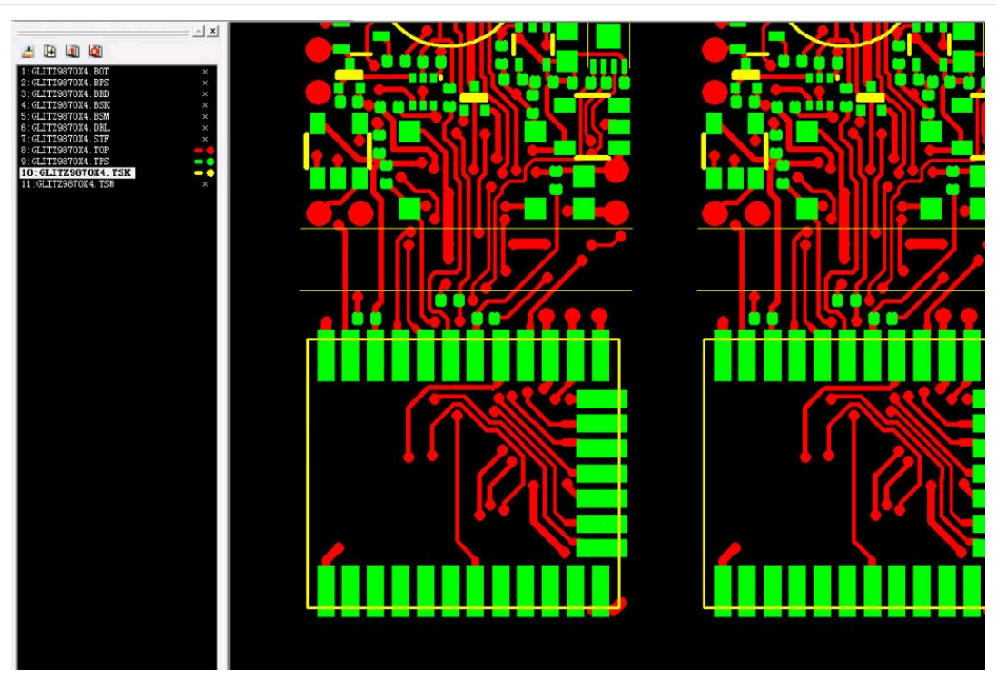
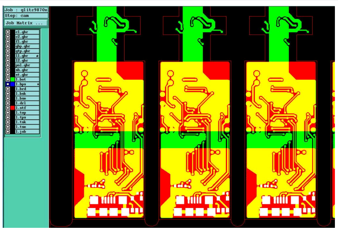
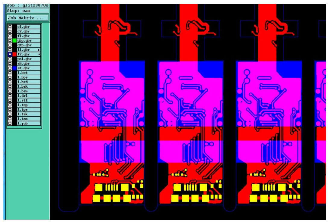
The first picture shows the top circuit side view, where SMD components can be seen on the bottom side. The second picture shows stiffeners (yellow area) designed for SMD components that should be assembled on the opposite side of the top; the design is nearly correct, but there are some SMD pads on the bottom side that are covered by stiffeners, which would be a mistake in the original design. The third picture shows the modified design for stiffeners (blue area) where the bottom stiffeners covering the SMD component area have been removed. The corrected design is ready to move to the manufacturing process.
The purpose of a flex circuit stiffener is to add a significant amount of functionality to your design and can be configured in an extremely wide range of combinations. All stiffener types can be combined in any flex PCB design. The mechanical nature of a stiffener’s function is one area of flex design that differs significantly from that of rigid printed circuit boards. This is a significant area in which design support is required to ensure that the finished parts meet their requirements.
1. What are the advantages of using flex versus cables?
Flex provides several advantages over cables. Flex’s higher upfront cost will dramatically reduce cost in the long run. Cables can take several weeks to go through production, while flex PCBs can be completed in several days. In short, using flex eliminates or decreases cable cost, reduces assembly time, and produces a lighter end product.
2. What are the preferred hole and pad sizes for flexible PCBs?
Flex material, such as polyimide, does not drill as well as regular materials. 10 mils and above is preferred for minimum size, only in the flex. Rigid-flex specs are similar to rigid board specs. The pad size and plating process for flex is barrel-only (hole wall). Flex holes are not plated on the surface because they need to flex, and because it is necessary to keep the electrodeposited copper off the surface.
3. Flex Prepreg Materials
No-flow prepreg is the preferred bonding material for joining flex and rigid materials. This is most commonly found in standard FR-4 or polyimide.
4. What are the alternative prepreg materials for joining flex and rigid materials?
No-flow prepreg is the preferred bonding material. Available in either standard FR-4 or polyimide.
5. What does a real stackup look like?
The plane layers for the flex are the same as they would be for the rigid board. This board would be turned into a 6-layer board, as follows:
A typical 6-layer flex stackup, from top to bottom, is constructed as follows:
Layer 1 (Top): Signal copper layer, covered by a flexible coverlay for protection
Layer 2: Ground plane
Layer 3: Signal routing layer
Layer 4: Signal routing layer
Layer 5: Power plane
Layer 6 (Bottom): Signal copper layer, covered by a flexible coverlay on the solder side
The copper layers are separated by polyimide dielectric cores and bonded with flex adhesive. As noted above, the plane layers for the flex are the same as they would be for the rigid board. Where the flex circuit joins a rigid section, no-flow prepreg is used to bond the two materials together.
Capabilities
Payment Methods


Specials Price
Carriers


Support Hobbyist
Certificate


Customer Support
Follow Us