 Knowledge Center
This Gold Phoenix PCB Knowledge Center article explains the Pin in Paste method, also called Through-Hole Reflow Technology, including component, PCB design, solder paste printing and inspection considerations.
The Pin in Paste method, also called through-hole reflow technology, has become increasingly important because it can increase automation while using existing manufacturing equipment.
Its advantages include:
Elimination of hand or wave soldering for applicable through-hole components
Reduction in manufacturing floor space
Reduction in manufacturing equipment and associated investment cost
Compatibility with existing processes
Possible use of a no-clean soldering process
Higher PCB-level reliability due to fewer soldering processes
Lower heating stress at the component level
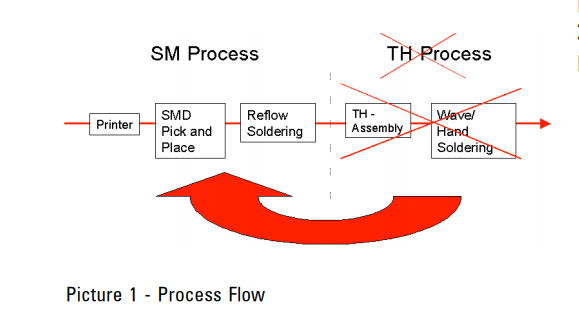
Through-Hole Reflow Technology provides a way to move suitable through-hole components into the surface-mount assembly process without losing the advantages of through-hole components. Extensive changes at the PCB and process levels may not be necessary.
When Through-Hole Reflow Technology is used, the surface-mount assembly process must be compatible with the specifications of the through-hole components. The main requirement is that the through-hole components withstand direct exposure to high temperatures during reflow soldering. Automatic pick-and-place handling and modifications to the solder paste printing process must also be considered.
With appropriate assembly-process modifications, solder-joint quality and long-term reliability can be maintained.
A conventional electronic-board assembly process can consist of two main component-placement and soldering steps.
During the first step, the PCB is populated with surface-mount components and soldered by reflow. During the second step, through-hole components are mounted and soldered by hand or wave soldering.
Eliminating the second step would require through-hole components to be replaced by equivalent surface-mount parts. However, equivalent surface-mount parts may not always be available, and electrical or mechanical limitations can also prevent such a substitution.
During wave soldering, heat reaches a through-hole component mainly by direct conduction through the wire leads.
With reflow soldering, the entire component, including the casing and terminals, must withstand temperatures up to 260°C for several seconds.
Components intended for automatic pick-and-place assembly can be supplied in standard packaging. For the fuse-type components discussed in this application, the tape width is 16 mm.
The tape structure keeps the leads positioned in the same direction to facilitate mounting, making component handling easier and reducing assembly time.
The construction of the component housing should allow visual inspection of the solder joint.
A stand-off pad underneath the component body is important to prevent contact between the component body and the solder paste during reflow.
A planar surface on top of the component also makes vacuum pickup at the center easier for pick-and-place equipment.
In the fuse-component design example, for a 0.6 mm pin diameter, a finished PCB hole diameter of 0.9–1.1 mm was identified as an optimum range.
The hole diameter is measured at the end of PCB manufacturing, including plating.
If the PCB hole diameter is too small, it becomes difficult to fill the hole properly with solder paste during printing. Low solder volume can cause a low-quality solder connection.
If the hole is oversized, too much solder may be required. Multiple printing steps may then be necessary to fill the oversized hole properly.
The required component lead length depends on PCB thickness.
An important consideration is whether the leads protrude through the bottom of the PCB. If the lead does not protrude, only one solder fillet forms on the top side and components on the bottom side are not affected.
Very long leads can push too much paste out of the hole, preventing the solder from flowing back properly to the solder joint during reflow.
If the lead is longer than the board thickness, the portion protruding from the bottom of the PCB should not exceed 1.5 mm.
One design example uses a PCB thickness of 1.55 mm with a component lead length of 1.4 mm.
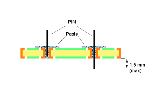
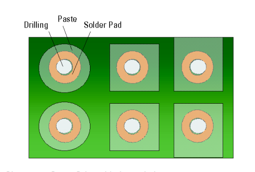
Overprinting and printing onto the PCB solder mask may sometimes be necessary to achieve the required solder paste volume.
Because of this, the solder paste should be compatible with the solder mask material. The preferred combination leaves no excess solder residue after reflow, allowing the solder to flow back to the solder joint.
Compatibility between solder paste and solder mask material should therefore be tested before implementing Through-Hole Reflow Technology.
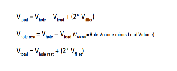
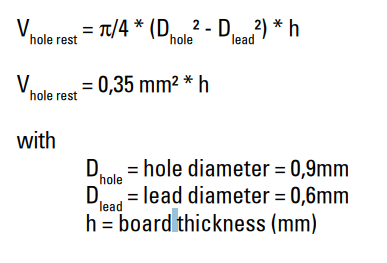
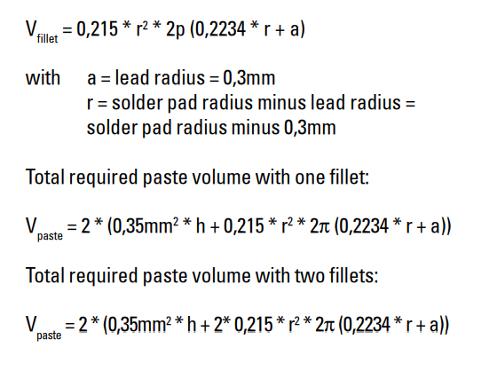
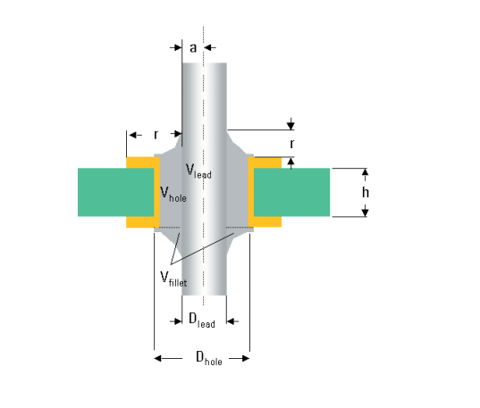
Solder paste contains about 50% metal material. The remaining material is released during the reflow process. Therefore, the required paste volume is approximately twice the calculated total solder volume:

The total required solder volume is based on the hole volume minus the lead volume, plus the required solder fillet volume.
If the lead does not protrude from the bottom of the PCB, one fillet is added. If the lead protrudes, two fillets are added.
Several methods can be used to dispense solder paste onto the PCB. Solder paste dispensers can press paste through special nozzles, while stencil printing is the most common method.
Stencil thickness depends on the lowest-pitch component on the PCB and can range from 75 μm to 300 μm.
The required solder paste volume can be controlled by changing the stencil aperture size. In general, the aperture must cover both the through hole and the solder pad.
The best results in the described process were obtained by printing twice onto the PCB without separating the PCB and stencil. During the second printing step, no additional paste is applied to the surface-mount pads, while solder paste flows deeper into the through holes.
Another approach uses two separate stencils. During the first step, solder paste for the through-hole components is forced into the holes. With the second stencil in place, additional paste is added to the holes, through-hole solder pads and surface-mount parts. This method requires two stencils and two printers.
A further approach uses a stepped stencil. Paste for the surface-mount components is printed first. During the second printing step, paste is applied into the holes using a second stencil with etched recesses on the bottom side. These recesses prevent the first print from being blurred.
Because many solder paste types are available, a single solder paste recommendation is not appropriate.
High viscosity is required during application. If the paste dries too quickly after printing, the component lead can press too much paste through the hole.
With low viscosity, the paste can become unstable and may not properly cover the hole.
The solder paste must therefore have suitable viscosity and robustness for the soldering process.
The inspection approach described for Pin in Paste solder joints uses visual inspection together with polished cross-section examination for non-visible areas.
The quality criteria include:
A minimum of 75% solder coverage on both sides of the wire leads
Less than 30% air cavities
100% wetting at the surface of the plated hole and on the component lead
The inspection criteria are based on IPC 610B Class B acceptance criteria for through-hole component solder joints.
Capabilities
Payment Methods


Specials Price
Carriers


Support Hobbyist
Certificate


Customer Support
Follow Us








