 Knowledge Center
This Gold Phoenix PCB Knowledge Center article explains via configurations for connecting decoupling capacitors to PCB power and ground planes, including opposite-direction current coupling, multiple-via arrangements, equivalent inductance, and plane current distribution.
This article focuses on the different via configurations that can be used to connect a decoupling capacitor to the PCB power and ground planes.
The inductance of the loop that connects a decoupling capacitor to a logic IC is of paramount importance and should be minimized. This article focuses on the different via configurations that can be used to connect a decoupling capacitor to the PCB power and ground planes. Small changes can significantly reduce the inductance of the decoupling loop.
A clocked digital IC usually needs large transient power supply currents. For example, a large microprocessor can draw currents as large as 10 A in a very short period of time. As the rise/fall time of the IC outputs decreases, this transient energy must be provided at a higher rate. The power and ground conductors of a PCB do exhibit some inductance. If the large transient current of the digital IC goes through the inductance of the power and ground conductors, there will be a voltage created across the inductance. Due to the large transient voltage drops across the power and ground conductors, a constant voltage cannot be delivered across the power and ground pads of the IC.
The solution to the above problem is to provide a source of charge that can provide the transient currents. This is usually achieved by placing decoupling capacitors very close to each logic IC. It is important to note that the circuit power routing only replenishes the charge in the decoupling capacitor and it is the decoupling capacitor that should supply all the high-frequency transient currents. A decoupling capacitor provides the transient currents in a short time interval associated with the rise/fall time of the IC outputs, and the power supply has at least half a clock cycle to recharge the decoupling capacitors. Keeping the high-frequency energy off the power distribution traces makes it easier to tolerate the unavoidable inductance of the power distribution structure.
As discussed above, decoupling capacitors are used to avoid supplying the high-frequency currents through the power distribution traces, which can exhibit a high inductance. That’s why the inductance of the path that connects the decoupling capacitor to the IC is important as well. If the inductance of the decoupling loop is not small enough, the logic IC will try to obtain some of its high-frequency energy through the power distribution structure. Therefore, the inductance of the decoupling loop must be carefully examined and minimized in every possible way. This article focuses on the different via configurations that can be used to connect a decoupling capacitor to the PCB power and ground planes.
The conventional method of mounting a decoupling capacitor is placing the vias next to the capacitor pads as shown in Figure 1.
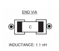
Figure 1
For this case, a typical value for the total inductance from the mounting pads of the capacitor to the power-ground plane pair is about 1.1 nH. To reduce the total inductance of these vias, the vias can be brought close together. Bringing the vias close together will increase the mutual inductance between them.
Since the currents of these two vias flow in opposite directions, the increased mutual inductance will reduce the net inductance of each via. To better understand this, remember that a current going through an inductor produces magnetic field lines that encircle the conductor. The direction of these magnetic field lines can be found by the right-hand rule shown below (in this example, the current direction is upward).
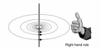
Figure 2
When the current goes through a via, it produces magnetic field lines that encircle it. Some of the magnetic field lines of one via will encircle the other via as well.
Since the two vias produce magnetic fields in the opposite direction (see Figure 3), the magnetic coupling between them will actually reduce the total number of field lines that encircle each via. The number of net magnetic field lines around a conductor determines its inductance. Therefore, when vias carry currents with opposite directions, increasing the magnetic coupling between them will reduce the effective inductance that each via exhibits.
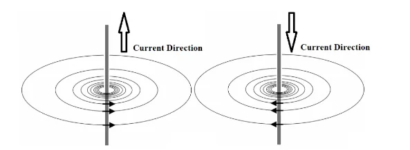
Figure 3
Therefore, one technique to reduce the inductance of the decoupling loop is to bring the vias close together as shown in Figure 4. In this case, the inductance between the mounting pad of the capacitor and the power-ground plane pair is reduced to 0.7 nH.
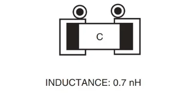
Figure 4
To further reduce the inductance of the decoupling loop, multiple vias can be used rather than using only one via for each capacitor pad. Two possible arrangements are shown in Figure 5.
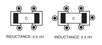
Figure 5
If there were no mutual inductance between the vias connected to the same pad, it could easily be concluded that the equivalent inductance of the parallel vias will be inversely proportional to the number of vias. What if there is some mutual inductance between them?
The currents through the vias connected to the same pad are in the same direction. Unlike the case in Figure 3, the magnetic coupling between the parallel vias of Figure 5 will increase the total number of field lines that encircle each via. Therefore, when vias carry currents with the same direction, increasing the magnetic coupling between them will increase the effective inductance that each via exhibits.
Consider the arrangement with two vias for each pad (the left figure above). Assume that the self-inductance of each via is L and the mutual inductance between the parallel vias is M (Figure 6 below). The equivalent inductance can be determined as follows:
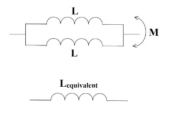
Figure 6
Considering the fact that the magnetic field lines of the two vias are in the same direction, it can be shown that the equivalent inductance of the two vias is given by:
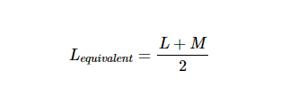
The mutual inductance, M, cannot be greater than the self-inductance L. Therefore, in the worst-case scenario, Lequivalent is close to L. However, if the vias connected to the same pad are placed sufficiently apart from each other, the mutual inductance M can be significantly reduced and an equivalent inductance close to L/2 can be obtained.
It is usually assumed that if the center-to-center spacing between the vias is greater than the length of a via, the mutual inductance becomes much less than the self-inductance. In this case, the equivalent inductance of the vias will be almost inversely proportional to the number of vias.
As noted above, with multiple vias, an equivalent inductance inversely proportional to the number of vias can be achieved. There is another mechanism that allows the arrangements of Figure 5 to have a lower inductance. To understand this second mechanism, the current distribution in a plane must be considered when the current is fed into or out of the plane through a via. As shown in Figure 7, in the vicinity of the vias, the current is constricted to flow into or out of the plane through a via. As the distance from the vias increases, the current can spread out.
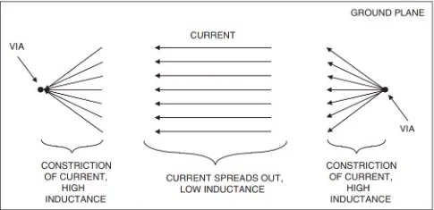
Figure 7
Examining the inductance of a plane can be a complicated problem and is beyond the scope of this article. The important point is that away from the vias the current can spread out and the plane exhibits a low inductance. However, near the vias the current cannot spread out and the inductance of the path increases significantly.
Interestingly, the total inductance of the current distribution shown in Figure 7 will be primarily determined by the large inductance in the vicinity of the vias. The arrangements of Figure 5 use several vias to connect to the planes. As a result, the multiple-via configuration allows the current to spread out in a wider area of the plane compared to the configurations that use a single via. Thus, multiple vias can reduce the inductance of the plane in the vicinity of the vias and, consequently, reduce the inductance of the decoupling loop.
Decoupling capacitors are used to avoid supplying high-frequency currents through power distribution traces, which can exhibit high inductance. If the inductance of the decoupling loop is not small enough, the logic IC will try to obtain some of its high-frequency energy through the power distribution structure. Therefore, the inductance of the decoupling loop must be minimized. This article discussed the different via configurations that can be used to efficiently connect a decoupling capacitor to the PCB power and ground planes. It was shown that vias with opposite-direction currents should be brought close together and that with appropriate spacing, a multiple-via configuration can lead to an equivalent via inductance that is inversely proportional to the number of vias. Another advantage of a multiple-via configuration is reducing the plane inductance in the vicinity of the vias.
Capabilities
Payment Methods


Specials Price
Carriers


Support Hobbyist
Certificate


Customer Support
Follow Us








