 Knowledge Center
PCB Design Guidelines for QFN Packages
This Gold Phoenix PCB Knowledge Center article presents general PCB design guidelines for mounting Quad Flat No-leads (QFN) packages, including PCB footprint, thermal via, solder mask and stencil considerations.
1.0 Scope
A QFN package is a near chip-scale plastic encapsulated (molded) or air-cavity package with a copper lead-frame substrate. Electrical contact to the PCB is made by soldering the lands on the bottom surface of the package to the PCB instead of using conventional formed perimeter leads.
The exposed die-attach pad or pads at the bottom of the package can effectively transfer heat to the PCB and provide stable electrical connections where applicable.
2.0 Terms and Definitions
· BSC — Basic Spacing between Centers, a term used on IC package drawings in reference to nominal dimensions.
· GaN — Gallium Nitride
· IEC — International Electrotechnical Commission
· IPC — Institute for Printed Circuits
· MSL — Moisture Sensitivity Level
· NSMD — Non-Solder Mask Defined
· Pb — Lead
· PCB — Printed Circuit Board
· PTH — Plated Through Hole
· QFN — Quad Flat No-leads
· REACH — Registration, Evaluation, Authorization and Restriction of Chemicals
· RoHS — Restriction of Hazardous Substances
· SMD — Solder Mask Defined
· Sn — Tin
3.0 General Design Note
These values are general PCB design guidelines rather than direct recommendations for every QFN design.
4.0 PCB Footprint Design Guidelines
For enhanced thermal, electrical and board-level performance, the exposed pads at the bottom of QFN packages need to be soldered to the PCB using a surface-mount process.
For proper heat conduction through the PCB, thermal vias need to be incorporated into the PCB in the thermal-pad region. PCB footprint design also needs to consider dimensional tolerances related to the package, PCB and assembly factors.
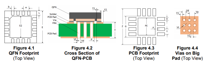
The following guidelines apply to PCB footprint and thermal-via dimensions in both the vertical and horizontal directions.
1. For good solder filleting, the PCB terminal pads should be 0.2 mm to 0.5 mm longer, away from the package center, than the package terminal length. The pads should also extend 0.05 mm toward the centerline of the package.
2. To minimize solder bridging, the pad width should equal the maximum width of the component terminal for lead pitches of 0.65 mm or less. If the pitch is more than 0.65 mm, the PCB pad can be 0.1 mm wider than the component terminal, adding 0.05 mm on each side.
3. To prevent solder bridging, the clearance between the terminal pads and the center pad or pads should be 0.15 mm minimum, with 0.2 mm recommended.
4. The minimum via drilling diameter is 0.2 mm. Diameters such as 0.2 mm, 0.25 mm, 0.3 mm and 0.33 mm can be used, with 0.3 mm recommended.
5. The minimum distance between the drilling edges of adjacent vias is 0.2 mm.
6. The minimum distance between the drilling edge of a via and the edge of the thermal pad can be 0.1 mm, with 0.2 mm recommended.
7. Typical copper plating thickness for the vias is 0.025 mm (1 mil) and can be increased to 0.050 mm (2 mils).
8. Terminal pads can be larger than the nominal footprint dimensions, and the same guidelines remain applicable to larger terminal pads. Vias can also be designed on larger terminal pads.
9. For vias with drilling diameters of 0.3 mm or less, it is normally not necessary to cover the vias with solder mask because solder mask may cause excessive solder voiding.
10. If via drilling diameters are greater than 0.3 mm, solder masking may be required to prevent solder wicking into the vias during reflow. Methods include via tenting from the top or bottom using dry-film solder mask, or complete or partial via plugging with conductive or non-conductive via-fill materials, depending on the power level and application. These additional processes increase PCB cost.
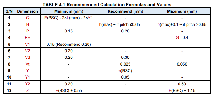
The recommended calculation formulas and values for the PCB footprint and thermal-via dimensions are summarized in the table below.
5.0 Solder Mask Design Guidelines
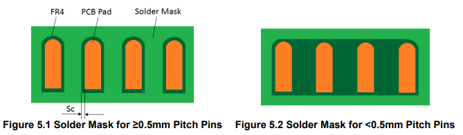
1. The clearance between the copper pad and the solder mask should be 0.015 mm to 0.020 mm. Typically, each pad can have its own solder mask opening for a lead pitch of 0.5 mm or higher. For finer-pitch devices, a common solder mask opening can be used. The inner edges of the solder mask should be rounded.
2. The thermal-pad area should be solder mask defined to help avoid solder bridging between the thermal pad and the perimeter pads. The mask opening should be 0.025 mm smaller than the thermal land size on all four sides.
6.0 Stencil Design Guidelines
1. A stencil thickness of 0.125 mm is recommended for devices with a pitch of 0.5 mm or less. A thickness of 0.15 mm to 0.20 mm can be used for parts with a pitch greater than 0.5 mm.
2. A laser-cut stainless steel stencil with electro-polished trapezoidal walls is recommended to improve solder-paste release.
3. To maximize solder-paste release, the stencil aperture should meet the following requirements:
Area Ratio = Area of Aperture Opening / Aperture Wall Area ≥ 0.66
Aspect Ratio = Aperture Width / Stencil Thickness ≥ 1.5
For rectangular aperture openings:
Area Ratio = LW / 2T(L + W)
Aspect Ratio = W / T
where L and W are the aperture length and width, and T is the stencil thickness.
4. The stencil aperture should be 1:1 to the PCB pad size or the area that needs to be soldered.
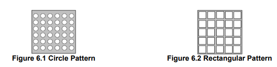
5. If the soldered area is large, such as 7 mm × 7 mm or greater, multiple smaller stencil openings are recommended instead of one large opening for printing solder paste, as shown below. Solder-paste coverage should be at least 50% for plugged vias and at least 75% for non-plugged vias.
Capabilities
Payment Methods


Specials Price
Carriers


Support Hobbyist
Certificate


Customer Support
Follow Us








