 Knowledge Center
Via tenting, via filling and via plugging are often confused in PCB design, but they serve different purposes and have different process requirements. This Gold Phoenix PCB Knowledge Center article explains the distinctions so designers can specify PCB requirements more clearly.
A via is a plated through hole (PTH) in a printed circuit board that provides an electrical connection between a trace on one PCB layer and a trace on another layer. Because a via is not used to mount component leads, it generally has a small hole and pad diameter.
Via tenting means covering the annular copper ring of a via with solder resist, also known as LPI (Liquid Photo Imageable) ink.
For via tenting, the solder mask opening at the via location is removed from the design so that solder resist covers the annular copper ring. The process does not necessarily guarantee that the surface of the via hole itself will be completely covered with solder resist.
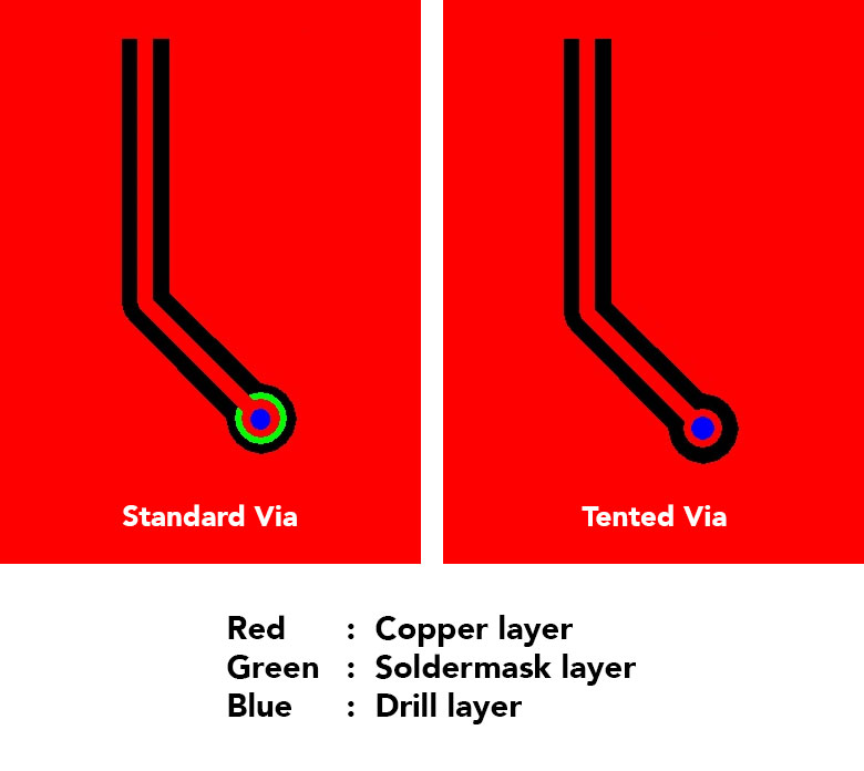
Standard via and tented via comparison.
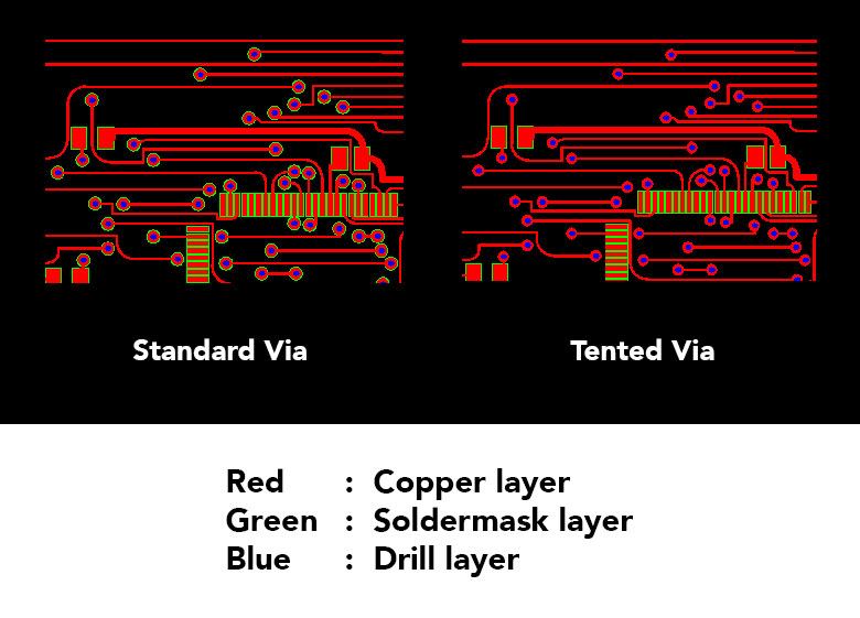
PCB layout comparison showing standard vias and tented vias.
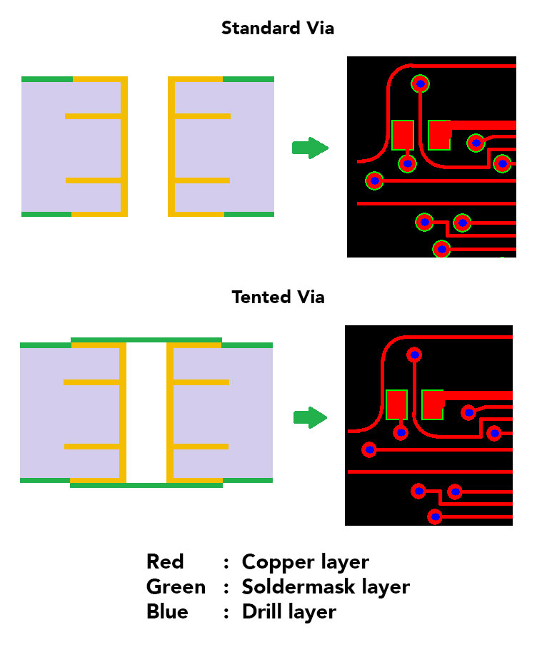
Cross-section comparison of standard and tented vias.
Via tenting is implemented through the solder mask process by removing the solder mask opening at the via location and covering the annular copper ring with solder resist.
Because via tenting relies on LPI solder mask over the via, the solder resist may not completely cover the surface of the hole. If the LPI layer over the via is broken, corrosive flux, moisture or other chemicals can enter and become trapped. This can increase the possibility of via failure as corrosion attacks the plated copper inside the barrel.
The use of no-clean flux in SMT assembly can reduce the possibility of contamination. However, corrosive water-clean flux used in through-hole assembly can still create problems. In this context, using a surface finish other than HASL can further reduce the risk.
In addition to tenting, via holes can be filled with solder resist ink (LPI). Two approaches described for this method are screen printing and filling through the normal solder mask process.
In the screen printing process, a drilled aluminum sheet is used to push standard solder resist ink into the via holes that need to be filled. The normal solder mask process is performed after the screen printing step.
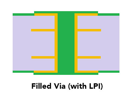
LPI-filled via cross-section.
Compared with relying on normal solder mask flow alone, this method is used when a more controlled via fill is required.
Less costly than conductive or non-conductive via plugging.
Suitable when the primary objective is to achieve a more consistently filled via.
Not suitable for Via in Pad applications or active vias.
When the solder mask opening is removed from the via location, solder resist ink can flow into the hole and over the annular ring during the standard solder mask process, potentially filling the via.
Via hole size has an important effect on the result. Via holes smaller than 0.3 mm have the best chance of being filled. For via holes between 0.3 mm and 0.5 mm, the filling result may vary depending on surface tension.
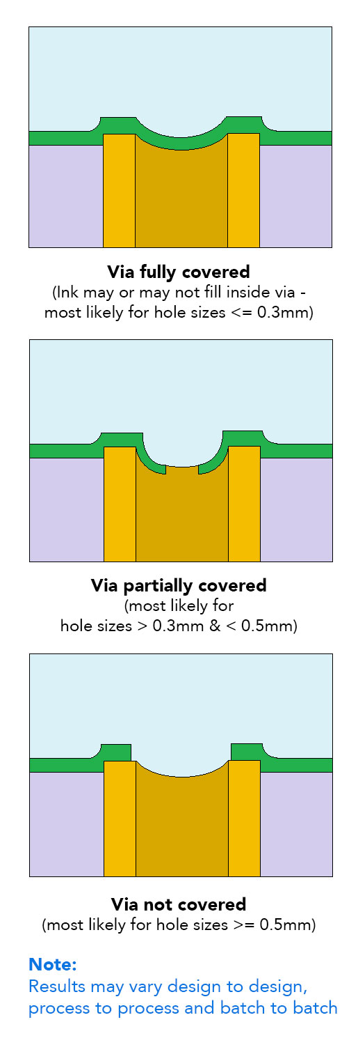
Via coverage examples for different hole sizes.
This approach uses the normal PCB solder mask process and does not require the separate screen-printing operation described above.
Not suitable when the design requires an assured completely filled via.
Not suitable for Via in Pad applications or active vias.
Therefore, it is not recommended for highly complex designs with fine-pitch BGA packages when a dependable filled-via result is required.
As electronic products become smaller and more advanced, PCB designers face increasing pressure to reduce board space without compromising performance. BGA packages with tighter spacing are therefore widely used.
Instead of using a standard “dog bone” footprint, where a signal travels from the BGA pad to a via and then to other layers, the via can be drilled directly into the BGA pad. This allows tighter routing because the surface of the via itself becomes part of the BGA pad and can be treated as a normal SMD pad for soldering.
This construction is known as Via in Pad, and the pad is referred to as an active pad.
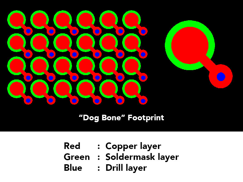
Dog-bone BGA footprint.
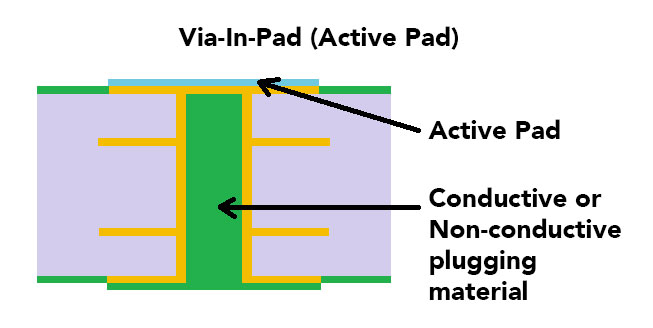
Via-in-Pad active pad cross-section.
There are two main types of via plugging based on the plugging material:
Non-conductive via plugging
Conductive via plugging
Of the two, non-conductive via plugging is the more commonly used method.
For PCB designs that need to transfer significant heat or current from one side of the board to the other, conductive via plugging can be used. It can also help dissipate excess heat generated beneath components. The metallic nature of the fill allows heat to move away from the component toward the opposite side of the board.
Can provide heat transfer where conventional methods are impractical, such as underneath a chip component.
The conductive fill material has a thermal conductivity of approximately 3.5 to 15 W/mK, which can increase current-carrying capacity compared with lower-conductivity filling material.
Conductive via plugging can create instability between the copper pad, the copper plating inside the via barrel and the surrounding laminate because of differences in coefficient of thermal expansion (CTE).
During PCB thermal cycling, the conductive fill can heat and expand more rapidly than the surrounding laminate. This can cause a fracture between the pad and the via barrel and may lead to an open circuit.
The thermal conductivity of conductive fill material is also much lower than that of electroplated copper, which has a thermal conductivity of more than 250 W/mK. In some designs, adding more vias may allow the use of the more reliable non-conductive via plugging approach instead.
Conductive via plugging is generally more expensive and less commonly used than non-conductive via plugging, and it may be offered by fewer PCB manufacturers.
Non-conductive via plugging is the more common method of via plugging, especially for Via in Pad applications.
The via barrel is filled with a specialized non-conductive plugging material. Material selection depends on factors such as CTE, availability, specific design requirements and the type of plugging equipment. The thermal conductivity of non-conductive plugging material is normally close to 0.25 W/mK.
A common misconception is that a via filled with non-conductive material will not carry current, or will carry only a weak electrical signal. This is incorrect. The via is plated normally before the non-conductive material is placed inside it, so the plated via continues to provide electrical connection in the same way as a standard via.
Prevents solder and other contaminants from entering the via.
Provides strength and structural support to active pads in Via in Pad applications.
Provides better pad and via stability and reliability because the CTE of the filling material more closely matches the surrounding laminate than conductive filling material.
Generally less expensive than conductive plugging because it is more widely used.
The lower thermal conductivity of non-conductive filling material makes it unsuitable for some designs.
The Via in Pad process consists of the following steps:
Drill the via as a through hole or blind via.
Fill the via with non-conductive material.
Plate the surface of the plugged via with copper.
Planarize the newly plated surface so that it is flat and even with the surrounding copper surface.
Apply the final surface finish, such as ENIG, ENEPIG or immersion silver.
The finished surface-mount pad is solderable and can also carry the signal to inner layers, eliminating the need to route the signal through a separate via.
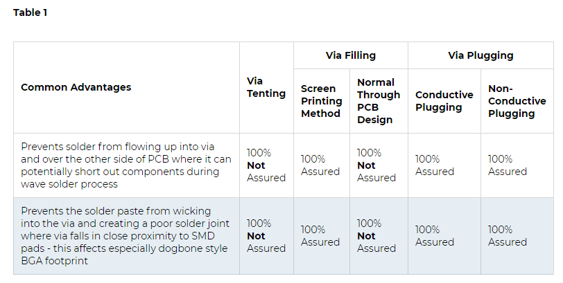
Comparison of common advantages for via tenting, filling and plugging methods.
Capabilities
Payment Methods


Specials Price
Carriers


Support Hobbyist
Certificate


Customer Support
Follow Us








