 Knowledge Center
Why is it necessary to define PCB trace clearance and pad clearance values?
High voltage/high current designs carry safety requirements which need to be met by designers. Similarly, high speed designs need to have suppressed crosstalk in order to ensure signal integrity. The key design aspects that relate to both areas are the PCB trace clearance and pad clearance values. These design choices are critical for balancing safety, noise suppression, and manufacturability.
IPC 2221 provides guidelines for conductor spacing and electrical safety considerations, but not all boards will need to meet this standard. Depending on the voltage and frequency of the signals (or edge rate for digital signals), a different value may be needed for the PCB trace clearance. This Gold Phoenix PCB Knowledge Center article explains how to balance these two aspects of the PCB layout while also ensuring manufacturability.
Under the IPC 2221 standards, the minimum PCB trace clearance (really, the clearance between any two conductors) is 0.1 mm for general purpose devices, or 4 mils. For power conversion devices, this minimum spacing is 0.13 mm, or 5.1 mils. These boards could hardly be considered “high voltage” and the conductor spacing in these boards starts to border on the HDI regime.
At these voltages, the design may be working with digital signals, low frequency analog signals, or simply DC at moderate current. With digital signals, the typical rule is to simply follow the “3W” rule, where the clearance between traces is triple the width of the trace. For a typical 50 Ohm controlled impedance microstrip, the trace width will be ~20 mils, thus the recommended trace spacing is 60 mils. These traces are still well within IPC 2221 requirements, and the primary focus should be efficient routing and DFM. Even in the HDI regime, where routing between fine-pitch pads in a BGA may be needed, these voltage requirements are generally not a concern when working at 3.3 V or ~1 V.
When the routing is this tight, the design is still well within PCB trace clearance requirements below 15 V. Instead, focus on signal integrity and DFM.
At high DC voltage, the primary concern in choosing a PCB trace clearance value is preventing ESD and dendritic growth between exposed conductors. With high AC voltage, or with a switching regulator that outputs high current, crosstalk must also be considered, as well as ESD and dendritic growth. Crosstalk suppression guidelines still over-specify the required voltage spacing between conductors until very high voltages are reached.
To see how a balance between IPC 2221 and crosstalk suppression may need to be found, consider the following hypothetical situation. Suppose there is a controlled impedance microstrip (20 mil wide) near a high voltage AC line, or near traces running in/out of a high current DC regulator. If the “3W” rule is followed, the spacing between parallel microstrips and the nearby high voltage line should be 1.5 mm, or ~60 mils. This is more than enough to comply with IPC 2221 until the high voltage level reaches 180 V for power conversion devices, or 340 V for other high voltage products.
At high voltage, the concern is not so much a digital edge rate as the frequency of a high voltage AC line. Any oscillating signal can induce a crosstalk signal in a nearby trace if the traces are close together; this is a known noise problem with high-voltage DC regulators and their downstream signal lines. At high output current, such crosstalk can induce unintended switching in high-speed digital components. It is best to opt for greater spacing between a high voltage AC line and nearby DC or digital lines.
If the PCB area is really limited, a 4mil pitch is barely acceptable. Therefore, when designing, it is important to consider the adaptability between the components, the PCB product and the product shell, and the space structure, reserving a safe distance for each target object to avoid spatial conflicts.
In PCB design, there are many places that need to consider the safety distance. Here, it is classified into two categories for the time being: one is electrical-related safety clearance, and the other is non-electrical-related safety clearance.
The minimum spacing between wires is 4mil. The minimum line distance is also the distance from trace to trace and trace to pad. From a production point of view, the larger the better if possible; the more common is 10mil.
Mechanically drilled pads use approximately 0.2mm, and laser-drilled structures use 4mil. The aperture tolerance can be controlled within 0.05mm, and the minimum pad width is 0.2mm.
The pad-to-pad spacing is 0.2mm.
The distance between the charged copper skin and the edge of the PCB board is preferably not less than 0.3mm. Set the spacing rules on the design-rules-board outline.
If it is a large area of copper, it usually needs to be retracted from the edge of the board, generally set to 20mil. In the PCB design and manufacturing industry, under normal circumstances, due to the mechanical considerations of the finished circuit board, or to avoid curling or electrical short-circuiting due to the exposed copper skin on the edge of the board, engineers often shrink a large area copper block by 20 mils relative to the edge of the board instead of spreading the copper to the edge of the board.
There are many ways to deal with this kind of copper shrinkage, such as drawing a keepout layer on the edge of the board, and then setting the distance between the copper paving and the keepout. Here is a simple method to set different safety distances for copper paving objects. For example, the safety distance of the whole board is set to 10mil, and the copper paving is set to 20mil, which can achieve the effect of 20mil shrinkage of the board edge, and also remove the dead copper that may appear in the device.
The text film cannot be changed during processing, but the character line width of D-CODE less than 0.22mm (8.66mil) is thickened to 0.22mm, that is, the character line width L=0.22mm (8.66mil).
The width of the entire character is W=1.0mm, the height of the entire character is H=1.2mm, and the spacing between the characters is D=0.2mm. When the text is smaller than the above standard, the processing and printing will be blurred.
Via-to-via spacing (hole edge to hole edge) is greater than 8mil.
The silk screen is not allowed to cover the pad. Because if the silk screen is covered with the pad, the silk screen will not be tinned during the tinning, which will affect the component mounting. A common PCB design reference is to maintain around 8mil clearance between silkscreen and pads. If the PCB board has a limited area, a 4mil pitch is barely acceptable. If the silk screen accidentally covers the pad during design, the board factory will automatically eliminate the part of the silk screen left on the pad during manufacturing to ensure that the pad is tinned.
Of course, specific conditions are analyzed in design. Sometimes the silk screen is deliberately close to the pad, because when the two pads are very close, the middle silk screen can effectively prevent the solder connection from shorting during soldering. This situation is another matter.
When mounting devices on the PCB, consider whether there will be conflicts with other mechanical structures in the horizontal direction and the height of the space. Therefore, when designing, it is important to consider the adaptability between the components, the PCB product and the product shell, and the space structure, reserving a safe distance for each target object to avoid spatial conflicts.
In general, PCB trace and pad clearance rules can be defined into three different regimes based on voltage, and two regimes based on whether it is electrical related safety clearance. In the two lower rows, be sure to calculate the required spacing using the IPC 2221 standard when determining which regime to work in. Note that the spacing can be made smaller when the traces are coated or are placed on inner layers.
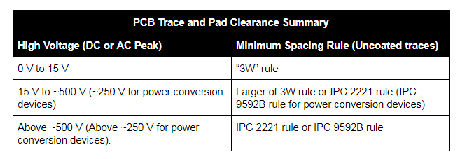
Be sure to understand the difference between creepage and clearance in the design. Also, be sure to check that the traces will be wide enough to carry sufficient current without becoming too hot. This can be checked using the IPC 2152 nomograph.
Once the best trace and pad clearances to use in the board have been figured out, these values need to be encoded as design rules in the ECAD software.
Capabilities
Payment Methods


Specials Price
Carriers


Support Hobbyist
Certificate


Customer Support
Follow Us








