 Knowledge Center
This Gold Phoenix PCB Knowledge Center article explains the four basic characteristics of RF circuits from four aspects: RF interface, small expected signal, large interference signal, and interference of adjacent channels. The important factors that need special attention in the PCB design process are given.
In concept, wireless transmitters and receivers are divided into two parts: fundamental frequency and RF. The fundamental frequency includes the frequency range of the input signal of the transmitter and the frequency range of the output signal of the receiver. The bandwidth of the fundamental frequency determines the basic rate at which data flows through the system. Baseband is used to improve the reliability of the data stream and reduce the load on the transmission medium imposed by the transmitter at a specific data transfer rate. Therefore, a lot of signal-processing engineering knowledge is needed when designing the PCB of a baseband circuit. The RF circuit of the transmitter converts the processed baseband signal, raise the frequency to the specified channel, and inject the signal into the transmission medium. In contrast, the receiver’s RF circuit takes the signal from the transmission medium and converts and reduces the frequency to the fundamental frequency.
Transmitters have two main PCB design objectives: the first is to achieve the required output power while maintaining efficient power consumption. Second, they must avoid interfering with the normal operation of transceivers in adjacent channels. In terms of receivers, there are three main PCB design objectives: first, they must accurately restore small signals; second, they must be able to remove interference outside the desired channel; finally, like transmitters, they must maintain low power consumption.
The receiver must maintain sensitivity to small signals, even in the presence of large interference signals. This occurs when an attempt is made to receive a weak or distant transmission that is broadcast on an adjacent channel by a powerful transmitter nearby. In some RF environments, interference signals are significantly stronger than the expected signal, reaching 60–70 dB above it, and they block reception of the normal signal through a large amount of coverage at the input stage of the receiver or by causing the receiver to produce excessive noise at the input stage. Both problems occur if the receiver is driven into a nonlinear region by an interference source during the input phase. To avoid these problems, maintain a highly linear receiver front end.
Therefore, “linearity” is an important consideration when designing a PCB receiver. Because the receiver is a narrow-frequency circuit, nonlinearity is calculated by measuring intermodulation distortion. This involves using two sinusoidal or cosine waves of similar frequencies in the central band to drive the input signal, and then measuring the product of their intermodulation. SPICE simulation requires significant computational resources for detailed RF analysis because many cycles are needed to achieve the required frequency resolution for observing distortion.
The receiver must be sensitive to small input signals. The input signal level of a receiver is very small, sometimes reaching microvolt-level signals. The sensitivity of the receiver is limited by the noise generated by its input circuit. Therefore, noise is an important consideration when designing a PCB receiver. The ability to predict noise with simulation tools is indispensable. The received signal is filtered and then amplified with a low-noise amplifier (LNA). The signal is then mixed with the first local oscillator (LO) to convert the signal to intermediate frequency (IF). The noise efficiency of the front-end circuit depends mainly on LNA, mixer, and LO. Although LNA noise is detected using traditional SPICE noise analysis, this approach is less useful for the mixer and LO because noise in these areas is severely affected by a large LO signal.
Small input signals require the receiver to be highly amplified. High gain levels such as 120 dB are required. At such a high gain, any signal coupled from the output back to the input will cause problems. An important reason for using the superheterodyne receiver architecture is that it distributes the gain over several frequencies to reduce the probability of coupling. This also makes the frequency of the first LO different from that of the input signal, preventing the large interference signal from contaminating the small input signal.
For different reasons, the superheterodyne architecture is replaced by direct-conversion or homodyne architecture in wireless communication systems. In this architecture, the RF input signal is converted directly to the baseband in a single step, so most of the gain is in the baseband, and LO is the same frequency as the input signal. In this case, understanding the impact of a small amount of coupling is critical, and a detailed model of the stray signal path must be established — such as coupling through the substrate, coupling between the encapsulation pins and the bondwire, and coupling through the power cord.
Distortion also plays an important role in the emitter. The nonlinearity of the transmitter in the output circuit causes the bandwidth of the transmitted signal to be spread over adjacent channels. This phenomenon is called spectral regrowth. The bandwidth of the signal is limited until it reaches the power amplifier (PA) of the transmitter. But intermodulation distortion in the PA causes bandwidth to increase again. If the bandwidth is increased too much, the transmitter will not be able to meet the power requirements of its adjacent channels. SPICE simulation has limitations when predicting spectral regrowth for complex digital modulation signals. Since about 1,000 symbol transmissions must be simulated to get a representative spectrum and combined with high-frequency carriers, this makes SPICE’s transient analysis impractical.
Because the RF circuit is a distributed-parameter circuit, skin effect and coupling occur during operation. In actual PCB design, radiation disturbance in the circuit is difficult to control, including mutual interference between digital and analog circuits, power-supply noise, and unreasonable grounding. Therefore, balancing the advantages and disadvantages and finding a suitable compromise point in PCB design is critical for reducing these interferences as much as possible or avoiding interference between some circuits.
For the whole RF circuit, RF units of different modules must be isolated with cavities, especially between sensitive circuits and strong radiation sources. In high-power multistage amplifiers, maintaining isolation between stages is required. After the whole circuit layout is placed, the shielded cavity must be treated with the following considerations.
Shielded cavities must be designed with regular shapes to simplify mechanical fabrication. For each individual cavity, rectangular shapes are required over square configurations.
The corners of shielded cavities must use arc shapes. Shielded metal cavities must use rounded corners for ease of manufacturing. See Figure 12.
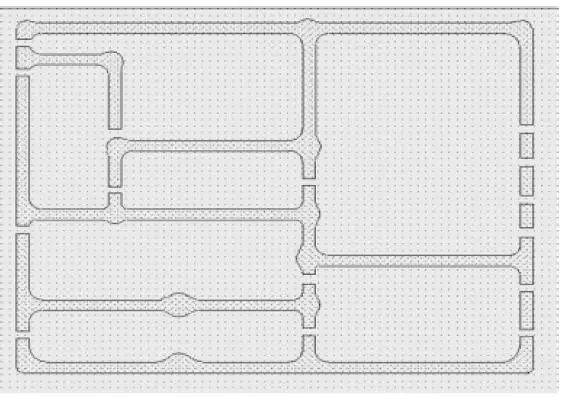
Figure 12. Cavity
The periphery of the shielded cavity is sealed, and the interface into the cavity adopts stripline or microstrip line, while the different modules inside the cavity adopt microstrip line, and the joint of different cavities adopts slot processing. The slot width is 3 mm, with the microstrip line routed through the center.
A 3 mm metallized hole is placed at the corner of the cavity to fix the shield shell, and similar metallized holes are placed evenly along each long cavity to reinforce the supporting function.
The cavity must be windowed to facilitate welding of the shielding shell. The thickness of the cavity must be more than 2 mm. Two rows of windows are added to the cavity, and the holes are staggered. The hole spacing is 150 mil.
Capabilities
Payment Methods


Specials Price
Carriers


Support Hobbyist
Certificate


Customer Support
Follow Us








