 Knowledge Center
Countless application cases of industrial, scientific and medical radio frequency (ISM-RF) products show that the printed circuit board (PCB) layout of these products is prone to various defects. When the same IC is installed on two different circuit boards, there will be significant differences in performance indicators. Changes in working conditions, harmonic radiation, anti-interference ability, and start-up time all illustrate the importance of circuit board layout in a successful design.
This Gold Phoenix PCB Knowledge Center article lists a variety of design oversights, explores the causes of circuit failures caused by each error, and gives suggestions on how to avoid these design flaws. This article takes FR-4 dielectric, a double-layer PCB with a thickness of 0.0625in as an example, and the bottom layer of the circuit board is grounded. The operating frequency is between 315MHz and 915MHz in different frequency bands, and the Tx and Rx power is between -120dBm to +13dBm. Table 1 lists some possible PCB layout problems, their causes, and their effects.
Table 1. Typical PCB layout issues and effects
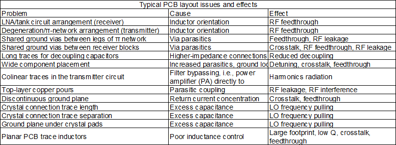
Most of these problems stem from a few common causes, and the following sections discuss them one by one.
When two inductors (or even two PCB traces) are close to each other, mutual inductance will occur. The magnetic field generated by the current in the first circuit will excite the current in the second circuit (Figure 1). This process is similar to the interaction between the primary and secondary windings of a transformer. When two currents interact through a magnetic field, the resulting voltage is determined by the mutual inductance LM:

In the formula, YB is the error voltage injected into circuit B, and IA is the current acting on circuit A. LM is very sensitive to circuit spacing, inductor loop area (that is, magnetic flux), and loop direction. Therefore, the best balance between a compact circuit layout and reduced coupling is the correct orientation of all inductors.
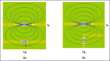
Figure 1. The mutual inductance is related to the inductor arrangement direction, as shown by the lines of magnetic force.
Adjust the direction of circuit B so that its current loop is parallel to the magnetic field lines of circuit A. To achieve this goal, place the inductors perpendicular to each other. A low-power FSK superheterodyne receiver evaluation (EV) board circuit layout demonstrates this principle (Figure 2). The three inductors (L3, L1, and L2) on the circuit board are very close. Arranging their directions as 0°, 45°, and 90° helps reduce the mutual inductance between each other.
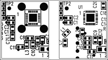
Figure 2. Two different PCB layouts — one with an unreasonable component arrangement direction (L1 and L3), and one more suitable.
Design requirements:
1. The inductor spacing should be as far as possible.
2. The inductors should be arranged at right angles to minimize crosstalk between inductors.
Just as the inductor arrangement direction affects the magnetic field coupling, if the leads are too close to each other, it will also affect the coupling. This layout problem produces mutual inductance. One of the most important concerns for RF circuits is the routing of sensitive components of the system, such as the input matching network, the receiver’s resonance tank circuit, and the transmitter’s antenna matching network.
The return current path must be as close as possible to the main current path to minimize the radiated magnetic field. This layout helps reduce the current loop area. The ideal low-resistance path for the return current is usually the ground area under the lead — effectively limiting the loop area to the dielectric thickness times the lead length. However, if the ground area is divided, it will increase the loop area (Figure 3). For the leads passing through the divided area, the return current will be forced to pass through a high-resistance path, which greatly increases the current loop area. This layout also makes the circuit leads more susceptible to mutual inductance.
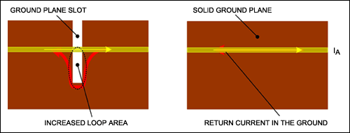
Figure 3. Complete large-area grounding helps improve system performance.
For an actual inductor, the lead direction has a great influence on the magnetic field coupling. If the leads of sensitive circuits must be close to each other, arrange the leads vertically to reduce coupling (Figure 4). If vertical arrangement is not possible, consider using a protection line. For the design of the protection line, refer to the grounding and filling treatment section below.
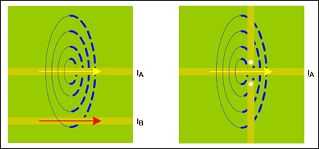
Figure 4. Similar to Figure 1, showing possible magnetic field coupling between adjacent leads.
Design requirements:
1. Ensure complete grounding under the lead.
2. Sensitive leads should be arranged vertically.
3. If the leads must be arranged in parallel, ensure sufficient spacing or use protective wires.
The main problem of RF circuit layout is usually that the characteristic impedance of the circuit is not ideal, including circuit components and their interconnections. The lead-wire copper layer is thinner, is equivalent to an inductance wire, and forms distributed capacitance with other adjacent leads. When the lead passes through the via, it also exhibits inductance and capacitance characteristics.
The via capacitance is mainly derived from the capacitance formed between the copper clad on the side of the via pad and the ground copper clad, separated by a relatively small ring. Another effect comes from the cylinder of the metal via itself. The influence of parasitic capacitance is generally small and usually only causes edge deterioration of high-speed digital signals (this article will not discuss this further).
The biggest impact of vias is the parasitic inductance caused by the corresponding interconnection method. Because in RF PCB design the size of most metal vias is the same as the size of lumped components, a simple formula can be used to estimate the influence of circuit vias (Figure 5):

In the formula, LVIA is the lumped inductance of the via; h is the height of the via, in inches; d is the diameter of the via, in inches.
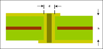
Figure 5. PCB cross-section via structure used to estimate parasitic effects.
Parasitic inductance often has a great influence on the connection of the bypass capacitor. The ideal bypass capacitor provides a high-frequency short circuit between the power plane and the ground plane, but non-ideal vias will affect the low-inductance path between the ground plane and the power plane. A typical PCB via (d = 10 mil, h = 62.5 mil) is approximately equivalent to a 1.34nH inductor. Given the specific operating frequency of an ISM-RF product, vias can cause adverse effects on sensitive circuits (for example, resonant tank circuits, filters, and matching networks).
If sensitive circuits share vias, such as the two arms of a π-type network, other problems will arise. For example, placing an ideal via equivalent to the lumped inductance, the equivalent schematic diagram is very different from the original circuit design (Figure 6). This is the same as the crosstalk of the shared current path, which leads to increased mutual inductance, increasing crosstalk and feedthrough.
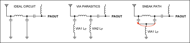
Figure 6. Comparison of ideal architecture and non-ideal architecture — there is a potential “signal path” in the circuit.
Design requirements:
1. Make sure to model via inductance in sensitive areas.
2. The filter or matching network should use independent vias.
3. Note that thinner PCB copper will reduce the influence of via parasitic inductance.
ISM-RF product data sheets often recommend using the shortest possible high-frequency input and output leads to minimize loss and radiation. This loss is usually caused by non-ideal parasitic parameters, so parasitic inductance and capacitance will affect the circuit layout, and using the shortest possible leads helps reduce parasitic parameters. Normally, a PCB lead with a width of 10 mil and a distance of 0.0625in from the ground plane, on an FR4 circuit board, will produce an inductance of about 19nH/in and a distributed capacitance of about 1pF/in. For LNA/mixer circuits with 20nH inductance and 3pF capacitance, the effective component value will be greatly affected when the circuit and component layout are very compact.
IPC-D-317A, published by the Institute for Printed Circuits, provides an industry-standard equation for estimating various impedance parameters of microstrip-line PCB. This document was replaced by IPC-2251 in 2003, which provides more accurate calculation methods for various PCB leads. Online calculators are available through various channels, most of which are based on the equations provided by IPC-2251.
The accepted standard for calculating the impedance of a microstrip line is:

In the formula, εr is the dielectric constant of the dielectric, h is the height of the lead from the ground, w is the lead width, and t is the lead thickness (Figure 7). When w/h is between 0.1 and 2.0 and εr is between 1 and 15, the calculation result of this formula is quite accurate.
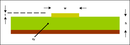
Figure 7. Cross section of the PCB (similar to Figure 5), showing the structure used to calculate the impedance of the microstrip line.
To evaluate the influence of lead length, it is more practical to determine the detuning effect of lead parasitic parameters on the ideal circuit. In this example, the discussion covers stray capacitance and inductance. The standard equation of characteristic capacitance for a microstrip line is:
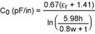
Similarly, the above equation can be used to calculate the characteristic inductance:

For example, suppose the PCB thickness is 0.0625in (h = 62.5 mil), 1 ounce copper-clad leads (t = 1.35 mil), the width is 0.01in (w = 10 mil), and an FR-4 circuit board is used. Note that the εr of FR-4 is typically 4.35 farads/meter (F/m), but it can range from 4.0F/m to 4.7F/m. The characteristic values calculated in this example are Z0 = 134Ω, C0 = 1.04pF/in, and L0 = 18.7nH/in.
For the ISM-RF design, a lead with a layout length of 12.7mm (0.5in) on the circuit board can produce parasitic parameters of approximately 0.5pF and 9.3nH (Figure 8). The effect of this level of parasitic parameters on the receiver’s resonant tank circuit (the change of LC product) may produce a change of 315MHz ±2% or 433.92MHz ±3.5%. Due to the additional capacitance and inductance caused by the lead parasitic effect, the peak value of the 315MHz oscillation frequency reaches 312.17MHz, and the peak value of the 433.92MHz oscillation frequency reaches 426.61MHz.
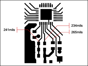
Figure 8. A compact PCB layout — parasitic effects will affect the circuit.
Another example is a resonant tank circuit of a low-power FSK superheterodyne receiver. The recommended components are 1.2pF and 30nH at 315MHz; 0pF and 16nH at 433.92MHz. The oscillation frequency of the resonant circuit is calculated using:

The resonant circuit of the evaluation board should include the parasitic effects of the package and layout. When calculating the 315MHz resonant frequency, the parasitic parameters are 7.3pF and 7.5pF respectively. Note that the LC product appears as a lumped capacitance.
Design requirements:
1. Keep the lead length as short as possible.
2. Place critical circuits as close as possible to the device.
3. Compensate key components based on actual layout parasitics.
The ground or power plane defines a common reference voltage, which supplies power to all parts of the system through a low-resistance path. In this way, all electric fields are balanced, resulting in a good shielding mechanism.
Direct current always tends to circulate along low-resistance paths. In the same way, high-frequency currents also preferentially flow through the lowest-resistance path. Therefore, for a standard PCB microstrip line above the ground plane, the return current tries to flow into the ground area directly below the lead. According to the lead coupling section above, a cut ground area will introduce various noises, which will increase crosstalk through magnetic-field coupling or current concentration (Figure 9).
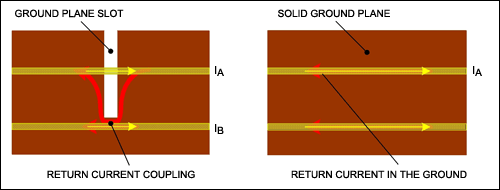
Figure 9. Keep the ground plane as complete as possible, otherwise the return current will cause crosstalk.
Filled ground is also called a protection line. It is usually used in circuits where it is difficult to lay a continuous grounding area or a design that needs to shield sensitive circuits (Figure 10). By placing grounding vias (that is, via arrays) at both ends of the lead or along the line, the shielding effect is increased. Do not mix the protective wire with the lead designed to provide a return-current path, as this layout will introduce crosstalk.
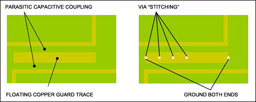
Figure 10. In RF system design, avoid floating copper-clad wire, especially when copper sheets need to be laid.
When the copper-clad area is not grounded (floating) or grounded at only one end, its effectiveness will be restricted. In some cases, it will form parasitic capacitance, change the impedance of surrounding wiring, or create a “potential” path between circuits, which will cause adverse effects. In short, if a piece of copper (non-circuit signal trace) is laid on the circuit board to ensure a consistent plating thickness, the copper-clad area should avoid floating because it will affect the circuit design.
Finally, consider the effects of any grounding areas near the antenna. Any monopole antenna regards the ground area, traces, and vias as part of the system balance. Non-ideal balanced wiring will affect the antenna’s radiation efficiency and direction (radiation pattern). Therefore, the ground area should not be placed directly under the monopole PCB lead antenna.
Design requirements:
1. Try to provide a continuous, low-resistance ground area.
2. Both ends of the filling line should be grounded, and via arrays should be used as much as possible.
3. Do not float the copper-clad wires near the RF circuit, and do not lay copper sheets around the RF circuit.
4. If the circuit board includes multiple ground layers, place a ground via when the signal line passes from one side to the other.
Parasitic capacitance will cause the operating frequency of the crystal oscillator to deviate from the target value. Some general guidelines must be followed to reduce the stray capacitance of crystal pins, pads, traces, or connections with RF devices.
Design requirements:
1. The connection between the crystal and the RF device should be as short as possible.
2. Keep the wires between each other as isolated as possible.
3. If the parallel parasitic capacitance is too large, remove the ground area under the crystal.
It is not recommended to use planar traces or PCB spiral inductors. Typical PCB manufacturing processes have certain inaccuracies, such as width and space tolerance, which greatly affect the accuracy of component values. Therefore, most controlled and high-Q inductors are wire-wound. Multilayer ceramic inductors are also an option. Nevertheless, some designers choose spiral inductors as a last resort. The standard formula for calculating planar spiral inductance usually adopts the Wheeler formula:

In the formula, a is the average radius of the coil in inches; n is the number of turns; c is the width of the coil core (rOUTER − rINNER), in inches. When c > 0.2a of the coil, the accuracy of this calculation method is within 5%.
Single-layer spiral inductors of square, hexagonal, or other shapes can be used. A very good approximation can be found to model the planar inductance on the integrated circuit wafer. To achieve this goal, the standard Wheeler formula was modified to obtain a planar inductance estimation method that is suitable for small size and square specifications:
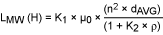
In the formula, ρ is the filling ratio; n is the number of turns; dAVG is the average diameter. For a square spiral, K1 = 2.36 and K2 = 2.75.
There are many reasons to avoid using this kind of inductance — it is limited by space and will lead to a reduction in inductance. The main reasons for avoiding planar inductors are restricted geometric dimensions and poor control of critical dimensions, which make it impossible to predict the inductance value. In addition, it is difficult to control the actual inductance value during the PCB production process, and the inductor also tends to couple noise to other parts of the circuit (see the lead coupling section above).
Design requirements:
1. Avoid using planar trace inductance.
2. Try to use wire-wound chip inductors.
Several common PCB layout pitfalls can cause ISM-RF design problems. However, by paying attention to the non-ideal characteristics of the circuit, these defects can be completely avoided. Compensating for these undesired effects requires proper handling of seemingly insignificant issues, such as component orientation, trace length, via placement, and grounding area usage. By following the guidelines above, significant time and money can be saved on correcting errors.
Capabilities
Payment Methods


Specials Price
Carriers


Support Hobbyist
Certificate


Customer Support
Follow Us








