 Knowledge Center
This Gold Phoenix PCB Knowledge Center article introduces Organic Solderability Preservatives (OSP) technology for printed circuit boards, covering how OSP protects bare copper, its benefits, the PCB OSP process, and the main defects of OSP finishes.
OSP is the abbreviation of Organic Solderability Preservatives and is also known as Preflux in English. Simply put, OSP forms a layer of organic protective film on a clean bare copper surface by chemical treatment. This film provides oxidation, heat-shock, and moisture resistance to protect the copper surface under normal environmental conditions from continued oxidation or sulfidization. During subsequent high-temperature soldering, the protective film must be readily removed by the flux so that the exposed clean copper surface quickly combines with molten solder to form a firm solder joint.
OSP is not a new technology; it is more than 35 years old, making it older than SMT. OSP offers benefits such as a flat surface, no IMC between the copper and solder pad, direct soldering of solder to copper during welding with good wettability, low-temperature processing, can be lower cost than HASL, and lower energy use during processing. OSP technology has been widely adopted in PCB manufacturing because of its surface protection and solderability characteristics. Early adoption in Japan was reported at about 40 percent of single-panel use and nearly 30 percent of two-layer panel use. In the United States, adoption increased from about 10 percent before 1997 to about 35 percent in 1999.
OSP has three main categories of materials: Rosin, Active Resin, and Azole. The azole type of OSP is currently the most widely used. Azole OSPs have undergone about five generations of improvement, named BTA, IA, BIA, SBA, and the latest APA.
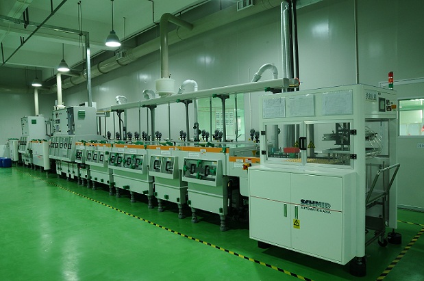
Oil removal → secondary water → microetch → secondary water → acid → DI water washing → film airing → DI water → dry
The oil removal effect directly affects film quality. Poor oil removal will result in non-uniform film thickness. The solution must be analyzed to control concentration within the process range, and the oil removal effect must be checked regularly. If the oil removal effect is not good, the oil removal fluid must be replaced in time.
The purpose of microetching is to form a rough copper surface to facilitate film formation. The thickness of micro-erosion directly affects the film-forming rate, so maintaining stable micro-erosion thickness is critical for achieving a stable film thickness. Control micro-corrosion thickness between 1.0–1.5 µm. The micro-corrosion rate must be measured before each production shift and used to determine the micro-corrosion time.
DI water is used for washing before film formation to prevent contamination of the film-forming solution. Washing after film formation also uses DI water, and the pH value must be controlled between 4.0 and 7.0 to prevent the film from being polluted or damaged.
The key to the OSP process is controlling the thickness of the anti-oxidation film. If the film is too thin, it has poor resistance to thermal impact. In over-reflow soldering, if the film is not resistant to high temperature (190–200°C), it will ultimately affect soldering performance. In an electronic assembly line, if the film cannot be well dissolved by flux, it will also affect soldering performance. The OSP coating thickness must be controlled at 0.2–0.5 µm.
OSP also has disadvantages. Formulation variations and performance differences exist between products. Process material selection must be appropriate to maintain stable OSP performance.
The protective film is very thin and easy to scratch, so boards must be handled carefully.
At the same time, after many high-temperature soldering processes, the OSP film on unsoldered connection pads becomes discolored or cracked, affecting solderability and reliability.
The solder paste printing process must be well controlled because a poorly printed board cannot be cleaned with IPA or similar methods without damaging the OSP layer.
The transparent and non-metallic OSP layer is difficult to measure for thickness, and its transparency makes coating coverage difficult to assess visually. These characteristics make visual inspection and thickness evaluation more challenging.
In OSP technology, there is no IMC isolation between the Cu of the solder pad and the Sn of the solder material. In lead-free technology, the SnCu in a solder joint with high Sn content increases rapidly, which affects solder-joint reliability.
Capabilities
Payment Methods


Specials Price
Carriers


Support Hobbyist
Certificate


Customer Support
Follow Us








