 Knowledge Center
This Gold Phoenix PCB Knowledge Center article explains common PCB panelization methods and key design considerations for panelized PCB assemblies.
After completing the PCB design of the entire board, the PCB needs to be mounted on the SMT assembly line to place components. Each SMT processing factory will specify the most suitable size of the PCB according to the processing requirements of the assembly line. If the size is too small or too large, the tooling for fixing the PCB on the assembly line cannot secure it properly. The solution is to combine multiple PCBs into one panel. Panelization can significantly improve efficiency for both high-speed placement machines and wave soldering. Multiple boards can be easily separated when doing panelization to avoid damage to the PCB during separation. The type of panelization method should be determined according to the shape of the individual board.
There are three main methods to panelize PCB boards: V-CUT, punching slot, and stamp hole. The size of the panel cannot be too large or too small. Generally, small boards are assembled or soldered in panels for convenience.
1. V-CUT
V-CUT means that several boards or the same boards can be combined and spliced together. After the PCB processing is completed, a V-shaped groove is cut between the boards with a V-CUT machine, which can be broken during use. This is the more popular method currently.
2. Punching Slot
Punching slot refers to milling out between the boards or inside the board with a milling machine as needed, which is equivalent to routing out the material.
3. Stamp Hole
The stamp hole method links boards together with small holes, which looks like the perforation on a stamp, hence the name. The stamp hole link requires high control of burrs on all sides between the boards — only one stamp hole can be used instead of the V line.
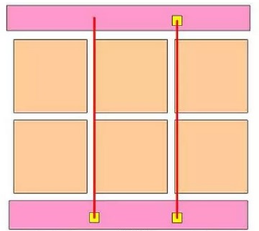
1. The outer frame (clamping side) of the PCB panel should adopt a closed-loop design to ensure that the PCB panel will not deform after being fixed on the fixture.
2. PCB board width ≤260 mm or ≤300 mm, depending on the assembly line specifications. If automatic dispensing is required, PCB board width × length ≤125 mm × 180 mm.
3. The PCB board shape should be as close as possible to square. It is recommended to use 2×2, 3×3, etc.
4. The center distance between the small boards should be controlled between 75 mm and 145 mm.
5. When setting the reference positioning point, a non-resist area 1.5 mm larger than the positioning point should be left around it.
6. There should be no large devices or protruding devices near the connection point between the outer frame and the inner small board, or between small boards. There should be more than 0.5 mm space between the components and the edge of the PCB board to ensure the normal operation of the cutting tool.
7. Four positioning holes should be made at the four corners of the frame, with a diameter of 4 mm ±0.01 mm. The strength of the holes should be moderate to ensure that they will not break during board handling. The precision of the hole diameter and position should be high, and the hole wall should be smooth and free of burrs.
8. Each small board in the panel must have at least three positioning holes, with a diameter of 3–6 mm. No wiring or components are allowed within 1 mm of the edge positioning hole.
9. The reference symbols used for the positioning of the entire PCB and the positioning of fine-pitch devices: in principle, the QFP with a spacing of less than 0.65 mm should be set at its diagonal position. The positioning reference symbols used for the panel daughter board should be paired and arranged at the opposite corner of the positioning element.
Capabilities
Payment Methods


Specials Price
Carriers


Support Hobbyist
Certificate


Customer Support
Follow Us








