 Knowledge Center
What is PCB?
Printed circuit boards (PCBs) are the boards that are used as the base in most electronics – both as a physical support piece and as the wiring area for the surface-mounted and socketed components. PCBs are most commonly made out of fiberglass, composite epoxy, or another composite material.
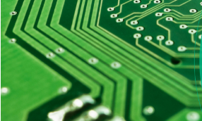
Most PCBs for simple electronics are simple and composed of only a single layer. More sophisticated hardware such as computer graphics cards or motherboards can have multiple layers, sometimes up to twelve.
Introduction
PCB (printed circuit board) is a printed circuit board, abbreviated as a printed circuit board, which is one of the important parts of the electronics industry. Almost every kind of electronic equipment, from electronic watches, calculators , to computers , communication electronic equipment, military weapon systems, as long as there are electronic components such as integrated circuits, in order to make the electrical interconnection between the various components must be printed plate. The printed circuit board is composed of an insulating bottom plate, a connecting wire and a pad for assembling and welding electronic components, and has the dual functions of a conductive circuit and an insulating bottom plate. It can replace complex wiring and realize the electrical connection between the various components in the circuit. It not only simplifies the assembly and welding of electronic products , reduces the workload of wiring in the traditional way, and greatly reduces the labor intensity of workers; it also reduces the overall machine Volume, reduce product cost, and improve the quality and reliability of electronic equipment. The printed circuit board has good product consistency, and it can adopt standardized design, which is conducive to the realization of mechanization and automation in the production process. At the same time, the entire printed circuit board that has been assembled and debugged can be used as an independent spare part to facilitate the interchange and maintenance of the entire product. At present, printed circuit boards have been extremely widely used in the manufacturing of electronic products.
The earliest printed circuit boards used paper-based copper-clad printed boards. Since the emergence of semiconductor transistors in the 1950s, the demand for printed boards has risen sharply. In particular, the rapid development and wide application of integrated circuits have made the volume of electronic equipment smaller and smaller, and the density and difficulty of circuit wiring have become greater and greater, which requires continuous updating of printed boards. At present, the variety of printed boards has developed from single-sided boards to double-sided boards, multilayer boards and flexible boards; structure and quality have also developed to ultra-high density, miniaturization and high reliability; new design methods, design supplies and Board-making materials and board-making techniques continue to emerge. In recent years, various computer-aided design (CAD) printed circuit board application software has been popularized and promoted in the industry. Among specialized printed board manufacturers, mechanized and automated production has completely replaced manual operations.
Although PCBs are most often associated with computers, they can be found in many other electronic devices, such as TVs, Radios, Digital cameras and Cell phones. In addition to their use in consumer electronics and computers, different types of PCBs are used in a variety of other fields, including:
Medical devices. Electronics products are now denser and consume less power than previous generations, making it possible to test new and exciting medical technology. Most medical devices use a high-density PCB, which is used to create the smallest and densest design possible. This helps to alleviate some of the unique constraints involved with developing devices for the medical field due to the necessity of small size and light weight. PCBs have found their way into everything from small devices, such as pacemakers, to much larger devices like X-ray equipment or CAT scan machines.
Industrial machinery. PCBs are commonly used in high-powered industrial machinery. In places WHERE current one-ounce copper PCBs do not fit the requirements, thick copper PCB can be utilized instead. Examples of situations where thicker copper PCBs would be beneficial include motor controllers, high-current battery chargers and industrial load testers.
Lighting. As LED-based lighting solutions catch on in popularity because of their low power consumption and high levels of efficiency, so too does aluminum-backed PCB which is used to make them. These PCBs serve as heat sinks and allow for higher levels of heat transfer than a standard PCB. These same aluminum-backed PCBs form the basis for both high-lumen LED applications and basic lighting solutions.
Automotive and aerospace industries. Both the automotive and aerospace industries make use of flexible PCB, which is designed to withstand the high-vibration environments that are common in both fields. Depending on specifications and design, they can also be very lightweight, which is a necessity when manufacturing parts for transportation industries. They are also able to conform to the tight spaces that might be present in these applications, such as inside instrument panels or behind the instrument gauge on a dashboard.
origin
The creator of PCB is Austrian Paul Eisler (Paul Eisler), in 1936, he first used a printed circuit board in the radio. In 1943, Americans mostly used this technology for military radios. In 1948, the United States officially approved this invention for commercial use. Since the mid-1950s, printed circuit boards have only begun to be widely used. Printed circuit boards appear in almost every electronic device. If there are electronic parts in a certain device, they are all mounted on PCBs of different sizes. The main function of PCB is to connect various electronic components to a predetermined circuit and play the role of relay transmission. It is the key electronic interconnection of electronic products and is known as the "mother of electronic products".
Features
The reason why PCB can be used more and more widely is because it has many unique advantages, which are roughly as follows:
Can be high-density
Over the years, the high density of printed boards has been able to develop correspondingly with the improvement of integrated circuit integration and the advancement of mounting technology.
High reliability
Through a series of inspections, tests and aging tests and other technical means, the PCB can be guaranteed to work reliably for a long time (usually 20 years).
Designability
The requirements for various properties of PCB (electrical, physical, chemical, mechanical, etc.) can be achieved through design standardization and standardization. In this way, the design time is short and the efficiency is high.
Manufacturability
PCB adopts modern management, which can realize standardization, scale (quantity) and automatic production, so as to ensure the consistency of product quality.
Testability
A relatively complete test method and test standard have been established. Various test equipment and instruments can be used to detect and appraise the eligibility and service life of PCB products.
Assemblability
PCB products are not only convenient for standardized assembly of various components, but also for automated and large-scale mass production. In addition, by assembling the PCB and various other components as a whole, larger parts and systems can be formed to the complete machine.
Maintainability
Since PCB products and various components are assembled in a standardized design and large-scale production, these components are also standardized. Therefore, once the system fails, it can be replaced quickly, conveniently and flexibly, and the system can be quickly restored to work.
PCB has other advantages, such as miniaturization and light weight of the system, and high-speed signal transmission.
Function
PCB has the following functions in electronic equipment.
(1) providing an integrated circuit and other electronic components is fixed, the mechanical support assembly, wiring and the electrical characteristics to achieve electrical connection between the integrated circuits and other electronic components connected to or electrically insulating, provided the required.
(2) Provide solder mask graphics for automatic welding, and provide identification characters and graphics for component insertion, inspection, and maintenance.
(3) After electronic equipment adopts printed boards, due to the consistency of similar printed boards, manual wiring errors can be avoided, and electronic components can be automatically inserted or mounted, automatic soldering, and automatic detection, ensuring electronic products The quality of the product improves labor productivity, reduces costs, and facilitates maintenance.
(4) Provide required electrical characteristics, characteristic impedance and electromagnetic compatibility characteristics for circuits in high-speed or high-frequency circuits.
(5) The printed circuit board with passive components embedded inside provides certain electrical functions, simplifies the electronic installation procedure, and improves the reliability of the product.
(6) In large-scale and ultra-large-scale electronic packaging components, an effective chip carrier is provided for the miniaturized chip packaging of electronic components.
Industry chain
Classified according to the upstream and downstream of the industry chain, it can be divided into raw materials, copper clad laminates, printed circuit boards, electronic product applications, etc. The relationship is as follows:
Fiberglass cloth: Fiberglass cloth is one of the raw materials for copper clad laminates. It is woven from glass fiber yarn and accounts for about 40% (thick board) or 25% (thin board) of the cost of the copper clad laminate. The glass fiber yarn is calcined into a liquid state from raw materials such as silica sand in a kiln. It is drawn into a very fine glass fiber through a very small alloy nozzle, and then hundreds of glass fibers are twisted into a glass fiber yarn. The construction investment of the kiln is huge, which generally requires hundreds of millions of funds, and once it is ignited, it must be produced 24 hours a day, and the cost of entry and exit is huge.
Copper foil: Copper foil is the raw material that accounts for the largest proportion of the cost of copper clad laminates, accounting for about 30% (thick plate) or 50% (thin plate) of the cost of copper clad laminates. Therefore, the price increase of copper is the main driving force for the price increase of copper clad laminates.
Copper clad laminate: The copper clad laminate is a product made by pressing glass fiber cloth and copper foil together with epoxy resin as a fusion agent. It is the direct raw material of printed circuit boards and is made after etching, electroplating, and multi-layer board pressing into a printed circuit board.
Capabilities
Payment Methods


Specials Price
Carriers


Support Hobbyist
Certificate


Customer Support
Follow Us








