 Knowledge Center
This Gold Phoenix PCB Knowledge Center article explains the surface treatment methods and design considerations for PCB gold fingers.
A gold finger (or edge connector) is created by inserting one end of the PCB into a connector slot, using the connector pin as the outlet for the external connection of the board. The pad or copper sheet contacts the pin at the corresponding position to achieve electrical continuity. Gold or nickel-gold is deposited on the pad or copper sheet of the board, and this is called a gold finger because of its finger shape.
1. Nickel-gold plating: The thickness can reach 3–50 μin. Because of its superior conductivity, oxidation resistance, and wear resistance, it is widely used on gold finger PCBs that need to be plugged in or mechanically rubbed frequently. However, because of the high cost of gold plating, it is only used for local gold plating such as gold fingers, also known as the selective gold plating process. The color of the gold plating process is silver-white, not as yellow as the immersion gold process. The disadvantage is that the solderability is slightly poor.
2. Immersion gold: The thickness is generally 1 μin, up to 3 μin maximum. Because of its superior conductivity, flatness, and solderability, it is widely used in high-precision PCB boards designed for key positions, wire-bonded ICs, BGAs, etc. For gold finger PCBs with low wear resistance requirements, the whole-board immersion gold process can also be chosen. The cost of the immersion gold process is much lower than that of the electroplating process. The color of the immersion gold process is golden yellow.
When a shape and package similar to the figure below is seen during PCB design, the first indication is that there are gold fingers on the board. Simple methods to identify gold fingers: devices with pins on the top and bottom surfaces; there will be a keying U-shaped slot as shown in the following figure.
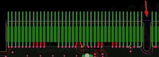
When there are gold fingers on the board, the details of the gold fingers need to be handled properly.
Gold finger detail processing in PCB:
For PCB boards that often need to be plugged in and out, gold fingers usually need to be plated with hard gold in order to increase their wear resistance.
The gold finger needs to be chamfered, usually at 45°, and other angles such as 20° or 30° are also possible. If there is no chamfer in the design, this is a problem. As shown in the figure below, the arrow indicates a 45° chamfer.
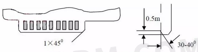
The gold finger requires all solder mask to be opened as a whole, and the pins do not need a stencil opening.
The minimum distance between solder/silver pads and the tip of the gold finger is 14 mil. It is recommended that the pad should be more than 1 mm from the gold finger position, including via pads.
The surface of the gold finger shall not be covered with copper.
All inner layers beneath the gold finger need copper clearance, usually 3 mm wide. Both half-finger copper clearance and full-finger copper clearance are acceptable. In PCIe design, it is also specified that the copper in the gold finger area should be removed completely.
The impedance of the gold finger is relatively low. Removing copper (clearing copper under the gold finger) can reduce the impedance difference between the gold finger and the impedance-controlled traces, and it also benefits ESD protection.
Recommendation: Fully clear copper under the gold finger pad.
Capabilities
Payment Methods


Specials Price
Carriers


Support Hobbyist
Certificate


Customer Support
Follow Us








