 Knowledge Center
With the continual development and progress of electronic technology, electronics products start developing towards the trends of light weight, thinness, miniaturization and advanced functions. After generations of upgrading, chip packaging technologies have led the ratio between chip area and package area to be approximately 1, among which BGA (ball grid array) has become a high-density packaging technology that has fallen into a pragmatic phase. This Gold Phoenix PCB Knowledge Center article discusses how to guarantee the reliability of BGA soldering quality, how to inspect the quality of BGA and how to implement rework on BGAs with defects — all of which are critical to BGA SMT (surface mount technology) assembly.
A BGA package contains lots of ball-shaped bumps at the bottom of the tube or at the upper surface. Thanks to the bumps, interconnection is achieved between the package body and the base. As an advanced packaging technology, BGA features large lead space and short leads through distributing I/O ends that perform as balls or columns at the bottom of the package body.
Based on different packaging materials, BGA components can be classified into PBGA (plastic BGA), CBGA (ceramic BGA), CCBGA (ceramic column BGA), TBGA (tape BGA) and CSP (chip-scale package).
Compared with QFP (quad flat package) components, BGA components feature the following properties:
a. I/O end spacing is so large that a higher number of I/O ends can be held by BGA.
b. Higher packaging reliability, lower soldering defects and more solid soldering joints.
c. BGA chips feature large spacing between soldering joints so that it is not difficult for alignment and soldering due to the alignment amplification system.
d. BGA soldering coplanarity is guaranteed as solder will automatically compensate for planarity error between chip and PCB after being melted.
e. Excellent electrical characteristics and frequency characteristics due to smaller soldering joints and low self-inductance and mutual inductance.
f. Capable in automatic self-alignment and tension between soldering joints leads to an excellent self-centering effect, causing high reliability.
g. The leading disadvantage lies in inspection and rework, which are relatively difficult to carry out.
A fishbone diagram indicating concerning elements in the manufacturing process of a PCB board containing BGA components is shown below.
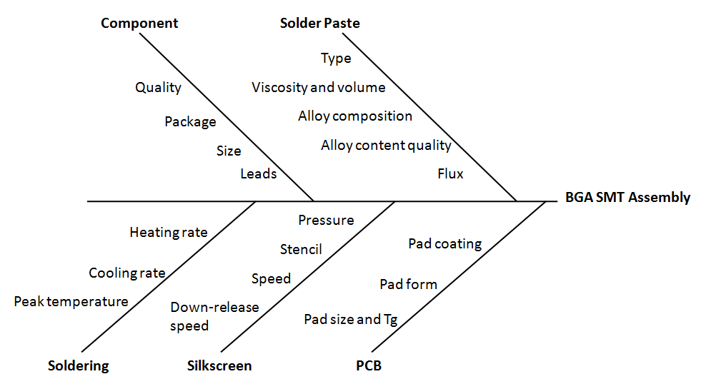
According to the above fishbone diagram, BGA SMT is closely associated with solder paste, components, PCB, silkscreen and soldering, among which soldering items are the most difficult to be dealt with in the reflow soldering process.
The key element affecting reflow soldering lies in temperature curve setting. The specific method is to open a hole at the position of some pad at the center of the BGA that is at the back side of the PCB and then lead a thermocouple probe through the hole from the bottom of the PCB board with it stuck to the backside of the pad and fixed with high-temperature tape. Next, a reflow soldering temperature curve tester with parameters well set is placed into the reflow soldering oven together with a tray and probe. After times of comparison and analysis, an optimal temperature curve will be obtained.
A reflow temperature curve consists of four phases: preheating phase, heat preservation phase, reflow phase and cooling phase. The heating process and temperature curve should make the package reach reflow temperature and then fall back to that of the pad after solder balls are melted with an intermetallic compound generated with the pad. Inconsistent heating will lead packages to unevenly fall or incline towards one side or corner of reflow soldering, causing non-coplanarity and inadequate soldering.
The following two aspects should be emphasized as well in terms of BGA soldering:
Plastic packaging usually absorbs humidity. If a chip is instantly heated after absorbing humidity in the air, moisture diffusion will lead to cavities inside the chip. As a result, the general baking condition of plastic packages is under 100°C for 6 to 8 hours.
Prior to their applications, BGA components should be inspected to ensure their pins are clean and have gone through no oxidation.
After soldering, BGA components possibly suffer from different defects due to components, assembly equipment, environment and soldering technologies. Leading BGA defects include misalignment, loose soldering, open circuits, cold soldering, bridging, short circuits and cavities. Furthermore, BGA solder balls possibly feature some issues as well, such as missing or falling and uneven sizes. When it comes to BGA inspection, it is definitely difficult to judge soldering quality after soldering because solder balls are below chips. Traditional visual inspection fails to determine whether defects or cavities are available inside soldering joints. Professional inspection equipment has to be used to clearly judge the quality of solder joints.
After BGA components are leveraged in SMT assembly, inspection methods that are usually relied on include electrical test, boundary scan and X-ray inspection. Traditional electrical test is capable of scanning open circuit and short circuit defects. Boundary scanning technology, depending on inspection ports designed based on boundary scanning, provides access to each solder joint on boundary connectors so that open circuits and short circuits can be inspected on components. Although boundary scan is capable of inspecting a wider range of invisible solder joints than electrical test, both methods only test electrical performance without reaching soldering quality inspection. To guarantee and improve the quality of the manufacturing process, other methods have to be relied on for soldering quality inspection, especially for those invisible solder joints.
Automated X-ray Inspection (AXI) can effectively solve this issue. AXI works on the principle that materials absorb X-rays according to their atomic weight proportion. Materials made of heavy elements absorb more X-rays, while those made of light elements absorb fewer. In a PCB assembly, solder joints are made of materials with heavy elements, while most packages, silicon ICs and component leads are made of materials with light elements. Therefore, high-quality solder joints appear darker or more obvious on X-ray images than other parts. This makes AXI particularly effective for inspecting components with array-style or fine-pitch packaging, including BGAs, CGAs (column grid arrays) and CSPs (chip-scale packages), where solder joints are hidden beneath the chip package and cannot be inspected by optical methods alone.
AXI is usually placed in the assembly process after the last soldering step, whether wave soldering or reflow soldering. For optimal inspection results, AXI is typically applied in combination with boundary scan test, in-circuit test (ICT) and functional test.
AXI features the following advantages as a type of structural test and inspection:
Some defects can be found in the early stage of the PCB assembly process
It contributes to the cost reduction of defects
It prevents defects from propagating to remaining assemblies or final products
AXI equipment is generally classified into two categories: 2D and 3D systems. Both types are responsible for inspecting manufacturing defects including open circuits, short circuits, insufficient solder, excessive solder, missing components, misaligned components and solder voiding.
Real-time monitoring can be carried out with AXI to ensure quality and provide real-time feedback for process control.
Optimal BGA soldering joints should be smooth, clear in boundary and void-free, and diameter, volume, grayscale and contrast should maintain the same among all the soldering joints with full alignment and no soldering balls generated. Compared with standards for optimal BGA soldering joints, qualified BGA solder joints feature a lower requirement.
Misalignment. An X-ray inspection device is capable of clearly indicating whether BGA solder balls are accurately compatible with pad positions on the PCB board. Less than 25% displacement can be allowed.
Loose Soldering Joints. No loose soldering joints are allowed for BGA soldering.
Open Circuits and Cold Soldering Joints. When solder does not contact the corresponding pad or solder features bad flowing, open circuits and cold soldering joints will possibly take place. Open circuits and cold soldering joints are not allowed for BGA soldering.
Bridging and Short Circuits. When solder is excessive or unsuitably placed, bridging and short circuits will possibly take place. As for BGA soldering joints, bridging and short circuits are not allowed.
Cavity. The issue concerning cavities is a little complicated. An X-ray inspection device is capable of demonstrating cavities on BGA component assemblies. The following tips are available as judgment standards:
1). Causes for Cavity Generation
① Cavities are available prior to soldering on BGA soldering balls, which possibly derive from solder ball manufacturing or solder paste constituents.
② If through holes are designed to be under the pad, external air will enter melting soldering balls through the holes with cavities formed after cooling.
③ The pad features bad coating or the pad surface is contaminated.
④ The reflow soldering temperature curve is unsuitably set.
2). Optimal Standard for Cavities
The air in cavities will possibly generate a stress effect of shrinkage and expansion. The place where cavities take place will be a stress focus, which is possibly the essential reason for stress cracks. BGA soldering joints with cavities will possibly lead to technical issues such as failure. According to the standard regulated by IPC on BGA soldering joints, cavities on the pad should not be larger than 10% of the solder ball area, that is, the diameter of cavities should not be larger than 30% of the solder ball diameter.
Capabilities
Payment Methods


Specials Price
Carriers


Support Hobbyist
Certificate


Customer Support
Follow Us








