 Centre de connaissances
This Gold Phoenix PCB Knowledge Center article explains ENIG black pad, why it can be difficult to detect on a bare printed circuit board, and the process factors associated with the failure mode.
When electroless nickel immersion gold (ENIG) was first being adopted more widely, black pad was difficult to identify because it was not usually evident on the bare printed circuit board. In many cases, the problem became apparent only after assembly.
At the time, many processes could become suspect, including the bare PCB, assembly, flux, solder and plating. The ongoing push toward RoHS compliance was forcing process changes in many areas without proper validation or verification of those processes. Immersion gold was becoming the lead-free surface finish of choice. At that time, ENIG was described as the most popular surface finish because of its outstanding reliability and flat finish.
The name black pad describes the appearance of the affected pads. Selected pads on one or both sides of a finished ENIG printed circuit board may appear partially or completely black after thermal processing during assembly.
Black pad is typically difficult to detect during bare PCB production.
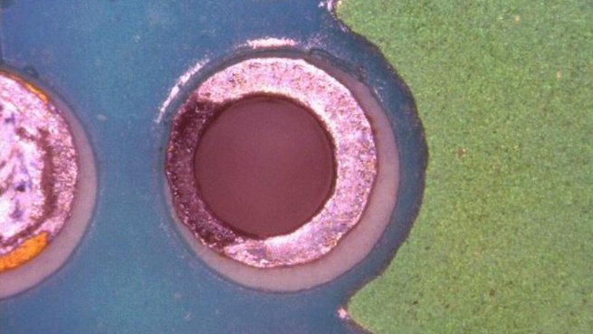
Black Pad quality issue on an immersion gold PCB.
The nickel beneath the gold becomes corroded, causing the surface to become brittle and separate during assembly processing. This can lead to cracked or failed solder joints that are not repairable and are often discovered too late, costing the industry millions in PCBs and components.
Reports and analyses at the time pointed to conditions in the nickel bath as the main cause of black pad, with excessive phosphorus identified as the primary issue.
Affected joints can break easily, exposing the corroded, blackened nickel beneath the surface.
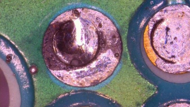
Close-up of a blackened pad observed on a PCB sample.
Even tightly controlled production environments that closely monitor chemistry levels, temperatures and incoming raw materials can experience this problem.
Multiple reflow processes during assembly have also been considered a possible contributor to black pad. Under these conditions, each reflow process can dissolve nickel and increase the ratio of phosphorus to nickel. If an ENIG-coated PCB begins with a phosphorus-to-nickel ratio within the recommended 7%–11% phosphorus composition, the dissolving of nickel during repeated reflow processes could increase the phosphorus composition beyond 11%.
Another possible cause of nickel corrosion is excessive immersion gold deposition. IPC guidance cited for the process recommends 2–4 micro-inches of gold deposition. The immersion gold process depends on nickel corrosion to complete the deposition. During the immersion process, nickel oxidizes and releases the electrons needed for gold to form a metallic coating on the nickel.
A requirement for a minimum of 3 micro-inches of gold can be difficult to meet consistently because the immersion process is self-limiting. Once all exposed nickel is covered, the immersion process stops.
To reach a 3 micro-inch minimum, the process may be accelerated through chemistry modifications so that gold deposits at a higher rate and produces a thicker deposit.
This can result in hyper-corrosion of the nickel surface and may initiate black pad.
Research and accumulated process data have led immersion gold chemistry suppliers and PCB manufacturers to improve materials and processes.
Process parameters can be set to minimize or even eliminate occurrences of black pad associated with the immersion gold process by avoiding the most well-documented causes.
← Back to How to Make a PCB
Capacités
Capacité PCB rigide
Capacité PCB flexible
Capacité d'assemblage PCB
Équipement PCB
Équipement d'assemblage PCB
Méthodes de paiement


Prix spéciaux
Transporteurs


Support pour amateurs
Certificat


Assistance clientèle
Suivez-nous


